Method of adding fabrication monitors to integrated circuit chips
a technology of integrated circuit chips and monitor devices, which is applied in the direction of originals for photomechanical treatment, semiconductor/solid-state device testing/measurement, instruments, etc., can solve the problems of limited scribe line area, continued shrinkage, and all desirable monitors not fitting in the available scribe line area
- Summary
- Abstract
- Description
- Claims
- Application Information
AI Technical Summary
Problems solved by technology
Method used
Image

Examples
first embodiment
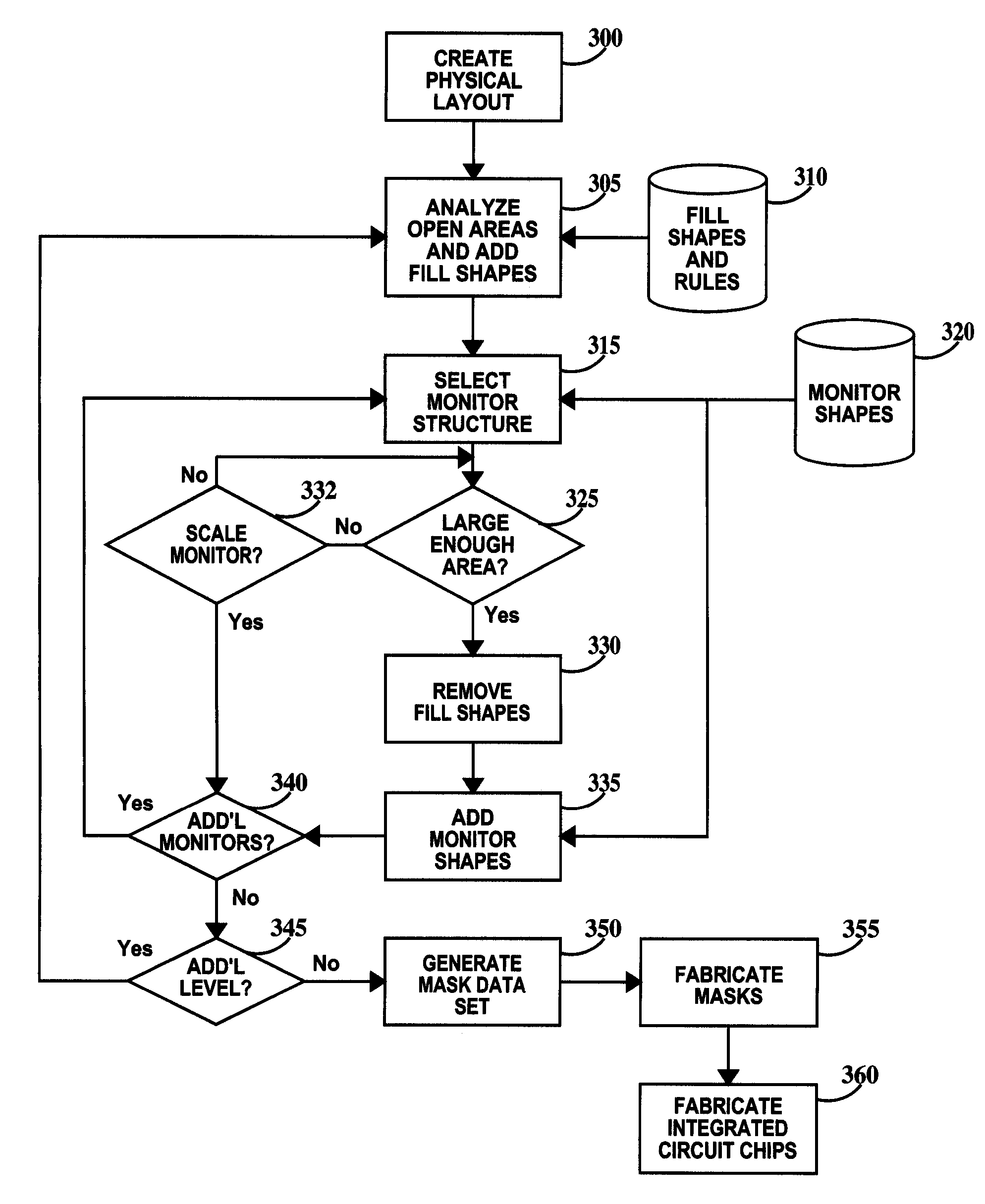
[0043]FIG. 10 is a flowchart of the present invention. In step 300. a physical layout file, called a shapes file is created, usually from a netlist. Shapes files are generated from netlist files which are a schematic representation of the circuits of the integrated circuits. Shapes files are a representation of the geometric shapes required to fabricate each of the photomasks required to fabricate all the levels of the integrated circuit and contain integrated circuit element shapes.
[0044]In step 305, open areas of the first or current photomask level, are analyzed and fill shapes selected and placed in the open areas based between integrated circuit element shapes based on fill shape selection and placement rules in a fill shapes and rules file 310. Examples of fill shape rules include, but are not limited to: the geometry and dimensions of the fill shapes, the minimum and maximum distances fill shapes can be placed from integrated circuit shapes, the distances between fill shapes ...
second embodiment
[0048]FIG. 11 is a flowchart of the present invention. Step 300 has been described supra in reference to FIG. 10. In step 370, areas between integrated circuit element shapes of the first or current photomask level, are analyzed. In step 375, the monitors to be inserted into the integrated circuit design are selected and blocks of open area are designated for placement of the shapes for each monitor structure based on the area requirement of each monitors' shape files listed in monitor shapes file 320. For monitor structures requiring more than one photomask level, a look-ahead may be performed to see if the required area in the proper position in the additional photomask levels exists as well. In step 380, the selected monitor fill shapes are placed in the blocks of area assigned to monitors. In step 385, fill shapes are placed based on the fill shape rules from fill shapes and rules file 310.
[0049]Next, in step 395, it is determined if any monitors are to be placed in the next pho...
PUM
 Abstract
Description
Claims
Application Information
 - R&D Engineer
- R&D Manager
- IP Professional
- Industry Leading Data Capabilities
- Powerful AI technology
- Patent DNA Extraction
Browse by: Latest US Patents, China's latest patents, Technical Efficacy Thesaurus, Application Domain, Technology Topic.
© 2024 PatSnap. All rights reserved.Legal|Privacy policy|Modern Slavery Act Transparency Statement|Sitemap