

Semiconductor device and manufacturing method thereof
a technology of semiconductor devices and manufacturing methods, applied in semiconductor devices, semiconductor/solid-state device details, instruments, etc., can solve the problems of difficult to achieve the desired wiring shape, difficult to achieve uniform discharge over the entire surface of one rectangular mother glass substrate, and difficult to narrow the distance between adjacent wirings. achieve the effect of not increasing the steps
- Summary
- Abstract
- Description
- Claims
- Application Information
AI Technical Summary
Benefits of technology
Problems solved by technology
Method used
Image

Examples
embodiment mode 1
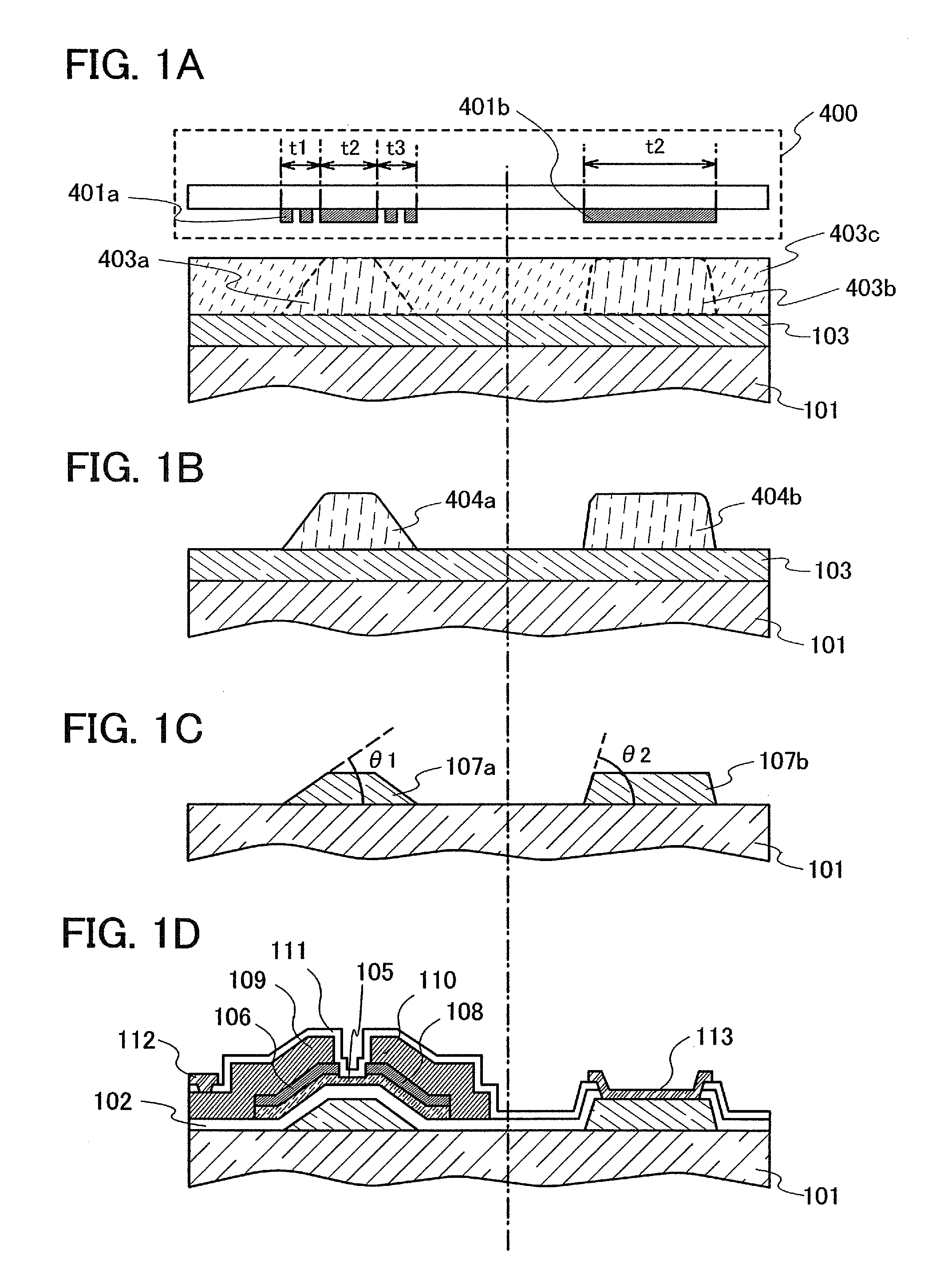
[0082]In this embodiment mode, a manufacturing process of forming, over the same substrate, a pixel portion having a thin film transistor and a terminal portion having a connection wiring for connecting it with an external device with the use of an FPC or the like is shown in FIGS. 1A to 1D.
[0083]First, a substrate 101 having an insulating surface is prepared. As the substrate 101 having an insulating surface, a light-transmitting substrate, for example, a glass substrate, a crystallized glass substrate, or a plastic substrate can be used. When the substrate 101 is a mother glass, any of the following sizes of the substrate can be used: the first generation (320 mm×400 mm), the second generation (400 mm×500 mm), the third generation (550 mm×650 mm), the fourth generation (680 mm×880 mm or 730 mm×920 mm), the fifth generation (1000 mm×1200 mm or 1100 mm×1250 mm), the sixth generation (1500 mm×1800 mm), the seventh generation (1900 mm×2200 mm), the eighth generation (2160 mm×2460 mm),...
embodiment mode 2
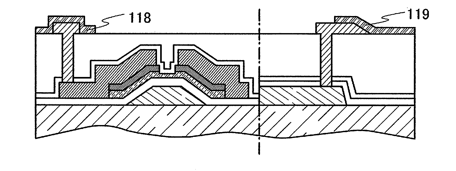
[0118]In this embodiment mode, an example will be described, in which cross-sectional shapes of a pixel portion and a terminal portion are made different at the time of forming a wiring over an interlayer insulating film which covers a thin film transistor, with reference to FIGS. 3A to 3D.
[0119]Note that since steps in the middle of a manufacturing process are the same as steps in Embodiment Mode 1, the detailed descriptions are omitted here. In addition, in FIGS. 3A to 3D, description will be made using the same reference numerals for the portions that are common to those in FIGS. 1A to 1D.
[0120]This embodiment mode shows an example of forming a planarization film over the insulating film 111 which covers the thin film transistor formed in Embodiment Mode 1.
[0121]First, steps up to and including the step of forming the insulating film 111 are performed in accordance with Embodiment Mode 1.
[0122]Next, a planarization film 114 is formed. The planarization film 114 is formed of an or...
embodiment mode 3
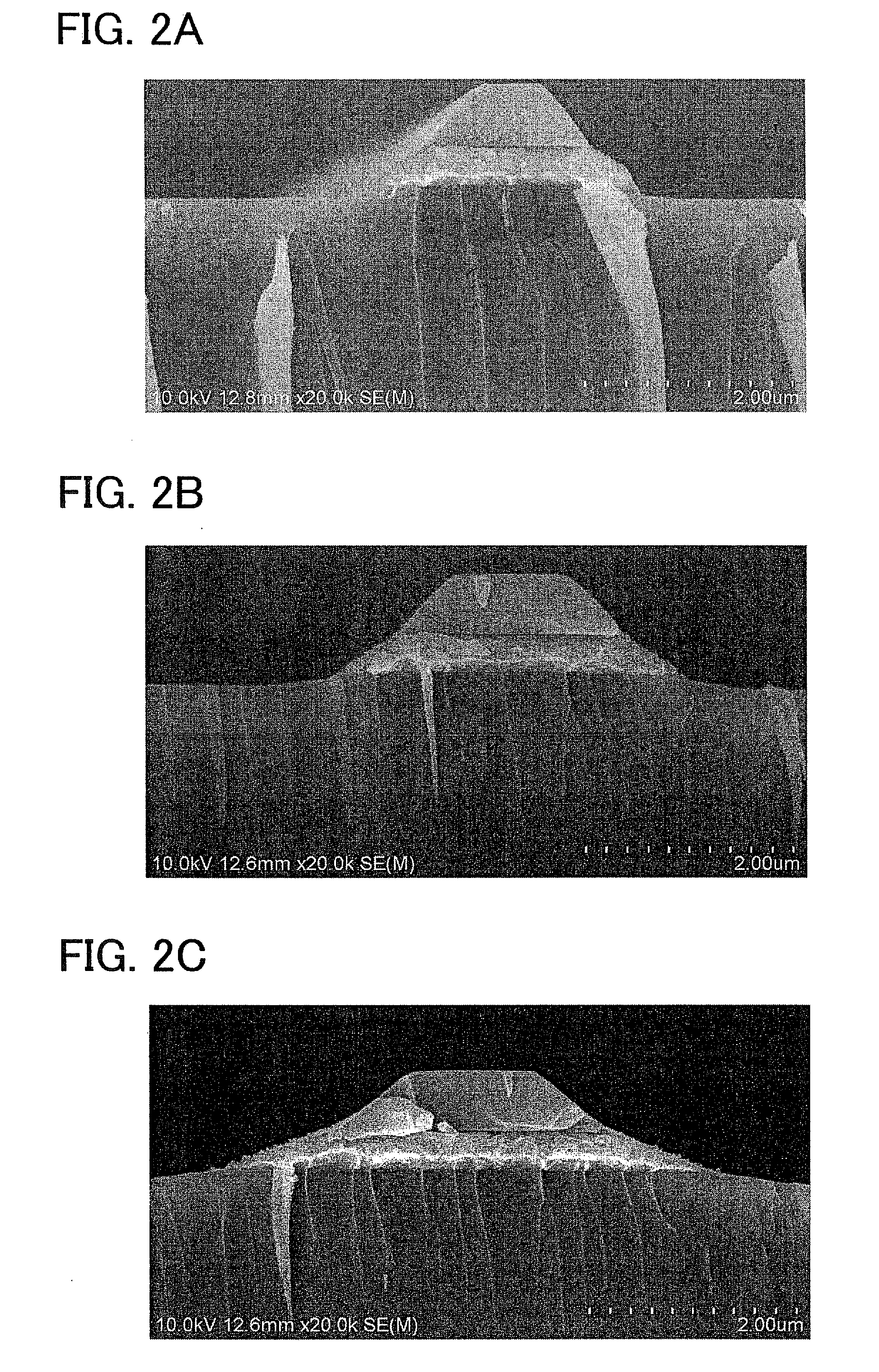
[0145]In this embodiment mode, a partially different example of Embodiment Mode 2 will be described with reference to FIGS. 6A to 6C. Since FIG. 6A is the same as FIG. 3A, the detailed descriptions are omitted here and the same reference numerals are denoted for the same portions.
[0146]In accordance with Embodiment Mode 2, steps up to and including the step of forming the third conductive layer 115 are performed, which are the same stage as FIG. 6A.
[0147]Next, the third conductive layer 115 is selectively etched using a photomask which is different from that of Embodiment Mode 2. In this embodiment mode, an example is shown in which a first connection electrode 120 having a taper angle only on one side is formed in a pixel portion, and a second connection electrode 121 having the same taper angle on both of the sides is formed in a terminal portion.
[0148]After the etching step described above, the remaining resist masks are removed by an ashing treatment or the like.
[0149]Next, afte...
PUM
 Abstract
Description
Claims
Application Information