Semiconductor device having stick drivers and a method of manufacturing the same

a technology of semiconductor devices and drivers, which is applied in the direction of semiconductor devices, instruments, optics, etc., can solve the problems of static electricity generation, limit in the reduction of manufacturing costs, and complicated work related to manufacturing

Inactive Publication Date: 2004-03-23
SEMICON ENERGY LAB CO LTD
View PDF63 Cites 174 Cited by
  • Summary
  • Abstract
  • Description
  • Claims
  • Application Information

AI Technical Summary

Problems solved by technology

Consequently, the work related to manufacturing becomes complicated, which is a problem.
However, there is also a limit in the reduction of manufacturing cost if the number of photomasks is not reduced.
Further, static electricity is generated by causes such as friction during manufacturing steps because the substrate is an insulator.
If static electricity is generated, then short circuits develop an intersection portion of wirings formed on the substrate, and deterioration or breakage of the TFT due to static electricity leads to display faults or deterioration of image quality in electro-optical devices.
In particular, static electricity develops during rubbing in the liquid crystal process performed in the manufacturing steps, and this becomes a problem.
In addition, if the number of pixels increases, then the number of IC chips installed will also inevitably become large.
The size of the IC chip is limited by the wafer size in the manufacturing process, and the practical size limit of the longer side is on the order of 20 mm.
A method of manufacturing a long size IC chip has also been considered, but the number of strip shape IC chips which can be cut out from a circular shape silicon wafer is naturally lowered, and therefore the method is not practical.
In addition, the silicon wafer itself has a fragile nature, and if a rather long IC chip is manufactured, then the probability of failures increases.
If the number of IC chips joined to one panel increases, then the likelihood of defects developing increases, which leads to a fear of reducing the yield.
In addition, the temperature coefficient of the silicon which becomes the substrate of the IC chip differs from the temperature coefficient of the glass substrate on which the pixel region is formed, and therefore problems such as warping develop after the two substrates are joined.
This becomes a cause of a lowering in the reliability of the element due to the developed mechanical stress, as well as of direct defects such as an increase in the contact resistance.
A large etching selectivity cannot be taken with this process, and consequently a portion of the first semiconductor film is also etched.
Further, there is also an error of 100 .mu.m in the positional alignment precision of markers formed on the substrate.
Therefore, it is necessary to have a 1 to 5 mm clearance in order to cut out stick drivers having a short side length of 2 mm using the glass scriber, and therefore there is a limit on how many stick devices can be taken from one substrate.

Method used


Image

  • Semiconductor device having stick drivers and a method of manufacturing the same
  • Semiconductor device having stick drivers and a method of manufacturing the same
  • Semiconductor device having stick drivers and a method of manufacturing the same

Examples


embodiment 1

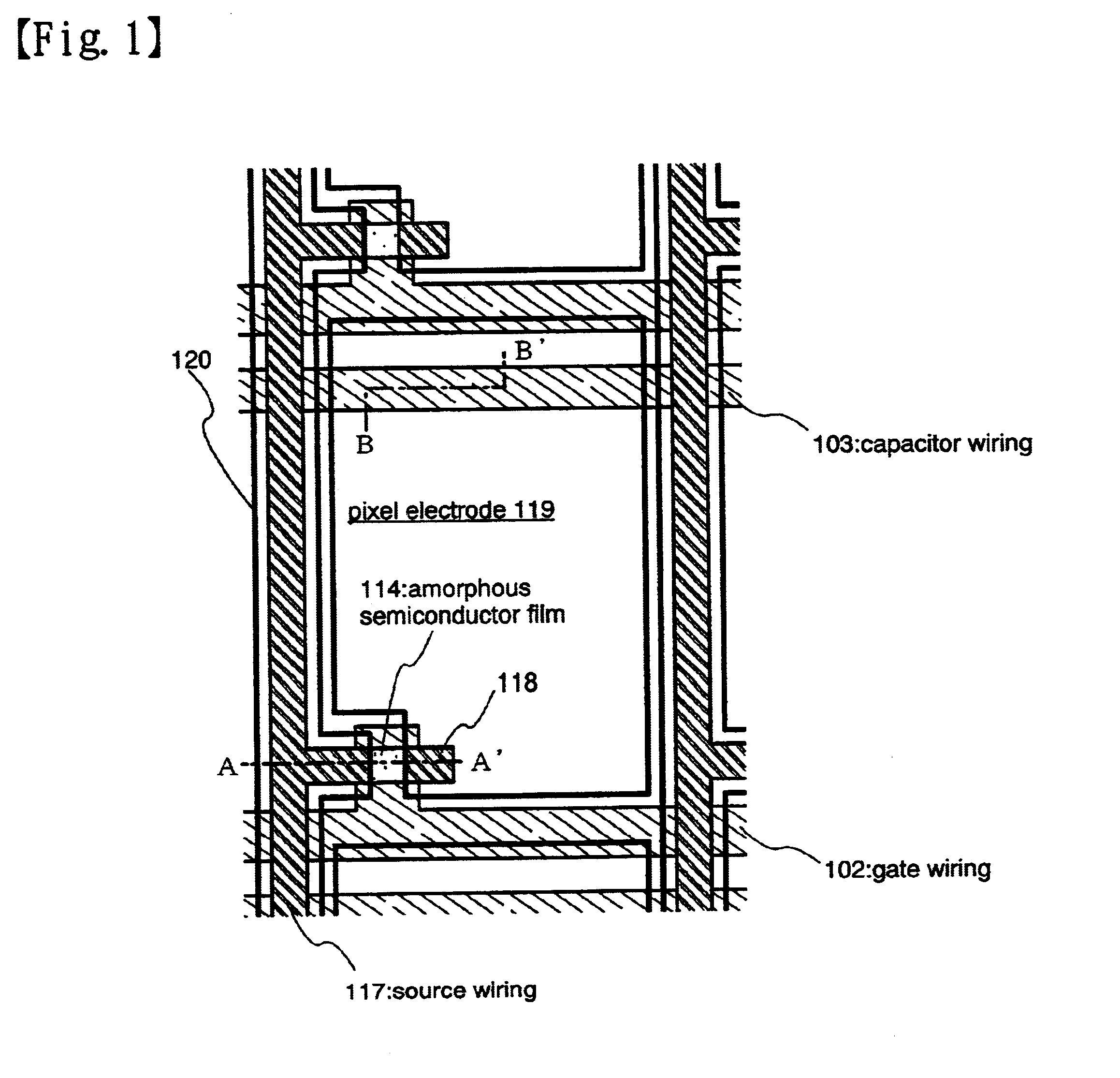
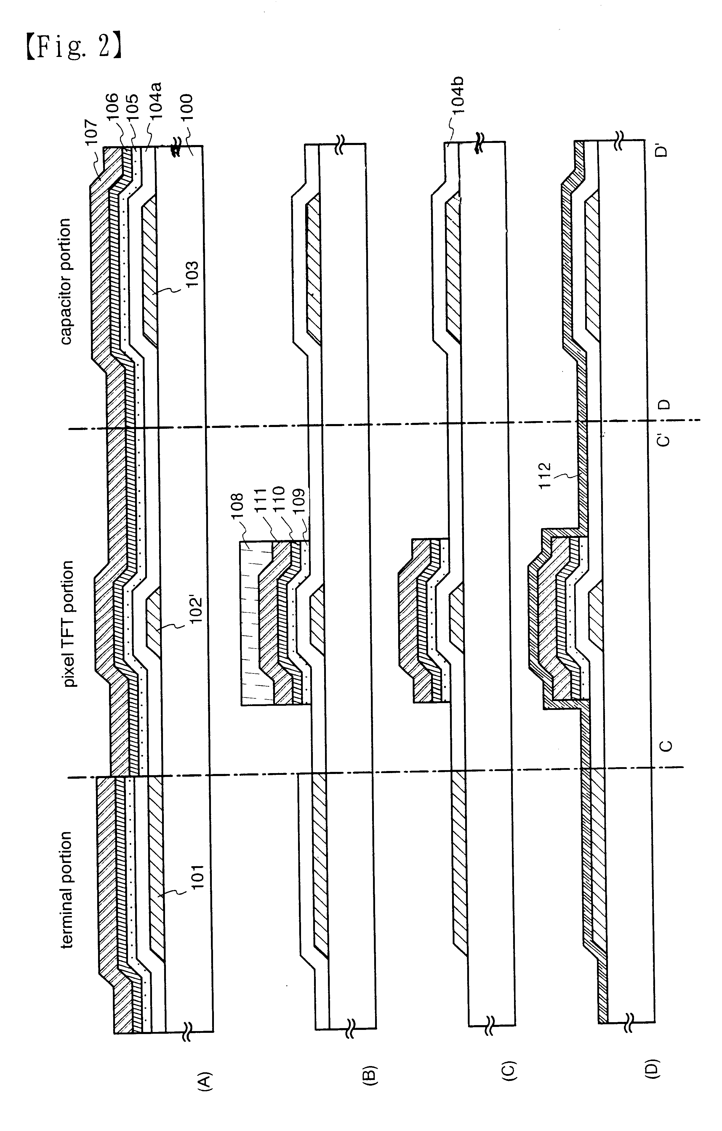
Embodiment 1 shows a method of manufacturing a liquid crystal display device, and a detailed explanation of a method of forming a TFT of a pixel portion on a substrate by a reverse stagger type TFT, and manufacturing a storage capacitor connected to the TFT, is made using FIGS. 1 to 5, in accordance with the processes used. Further, a manufacturing process for a terminal portion, formed in an edge portion of the substrate, and for electrically connecting to wirings of circuits formed on other substrates, is shown at the same time in the same figures.

In FIG. 2(A), a glass substrate, such as a barium borosilicate glass substrate or aluminum borosilicate glass substrate, typically Coming Corp. #7059 or #1737, is used as a substrate 100. In addition, a substrate such as a quartz substrate or a plastic substrate can also be used.

After forming a conductive layer over the entire surface of the substrate 100, a photolithography process using a first photomask is performed, and etching proce...

embodiment 2

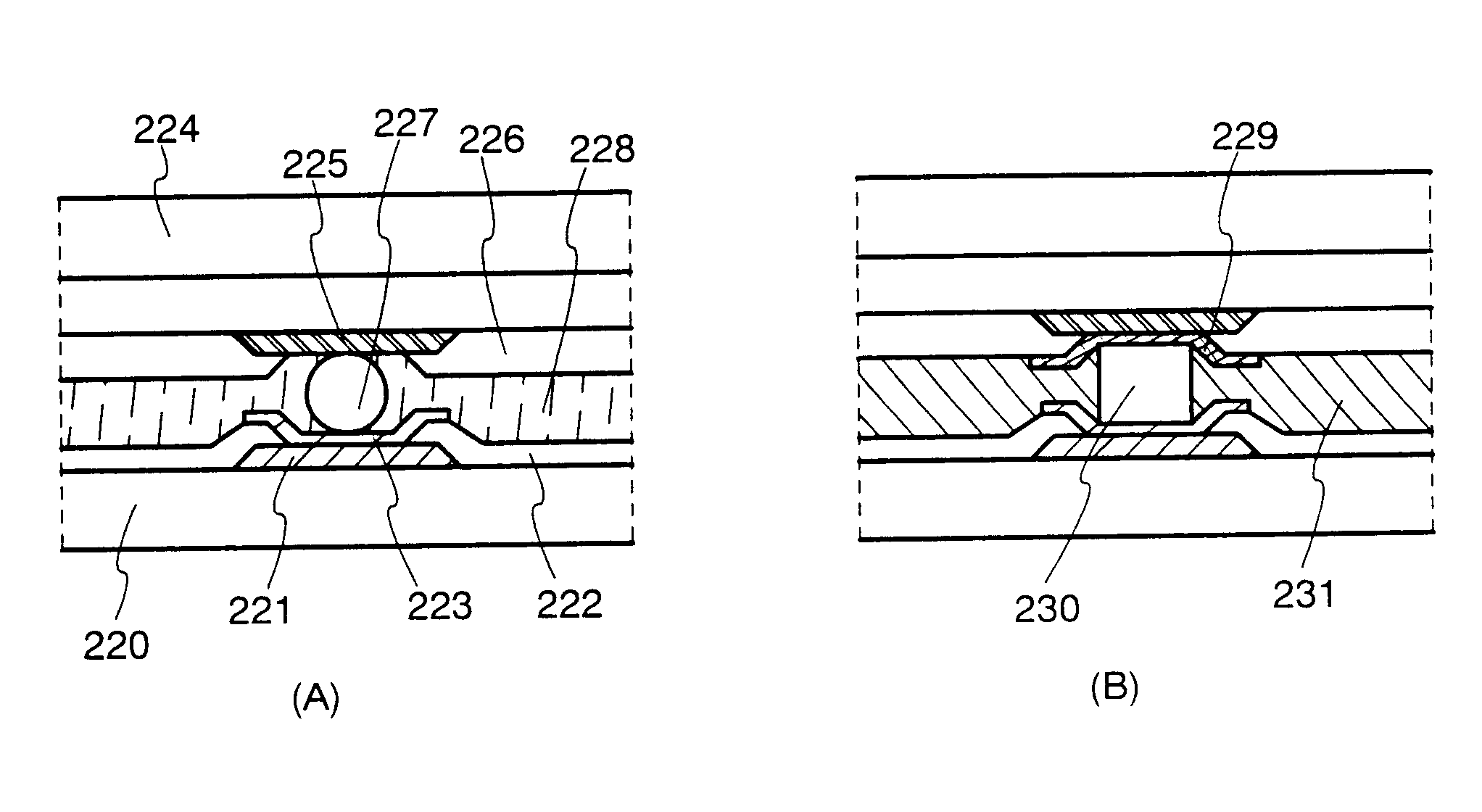
In Embodiment 2, an example of forming a protecting film on the pixel TFT manufactured in Embodiment 1 is shown in FIG. 12. Note that Embodiment 2 is identical to Embodiment 1 through the state of FIG. 3(B), and therefore only points of difference are explained. Further, the same symbols are used for locations corresponding to those in FIG. 3(B).

After first forming through the state of FIG. 3(B) in accordance with Embodiment 1, a thin inorganic insulating film is formed on the entire surface. An inorganic insulating film such as a silicon oxide film, a silicon nitride film, a silicon nitride oxide film, or a tantalum oxide film is used as the thin inorganic insulating film, and a single layer or a lamination structure made from these materials may be formed.

A photolithography process is performed next using a fourth photomask, forming a resist mask, and unnecessary portions are removed by etching, forming an insulating film 402 in the pixel TFT portion, and an inorganic insulating f...

embodiment 3

In Embodiment 1 an example centering on forming an insulating film, a first amorphous semiconductor film, a single conductivity type second amorphous semiconductor film, and a first conductive film by sputtering, but Embodiment 3 shows an example of using plasma CVD to form the films. Specifically, the insulating film, the first amorphous semiconductor film, and the single conductivity type second semiconductor film are formed by plasma CVD.

A silicon nitride oxide film is used as the insulating film in Embodiment 3, and is formed with a 150 nm thickness by plasma CVD. At this time, the power source frequency in the plasma CVD device is from 13 to 70 MHz, preferably between 27 and 60 MHz. In particular, by using a power source frequency of 27 to 60 MHz, a dense insulating film can be formed, and as a gate insulating film, the voltage resistance can be increased. Further, a silicon nitride oxide film manufactured by adding SiH.sub.4, NH.sub.3, and N.sub.2 O has a relaxed stress in the...


PUM

PropertyMeasurementUnit
sizeaaaaaaaaaa
lengthaaaaaaaaaa
lengthaaaaaaaaaa

Abstract

A pixel TFT formed in a pixel region is formed on a first substrate by a channel etch type reverse stagger type TFT, and patterning of a source region and a drain region, and patterning of a pixel electrode are performed by the same photomask. A driver circuit formed by using TFTs having a crystalline semiconductor layer, and an input-output terminal dependent on the driver circuit, are taken as one unit. A plurality of units are formed on a third substrate, and afterward the third substrate is partitioned into individual units, and the obtained stick drivers are mounted on the first substrate.

Description

1. Field of the InventionThe present invention relates to a semiconductor device having a circuit composed of a thin film transistor (hereafter referred to as TFT), and to a method of manufacturing thereof. In particular, the present invention relates to the structure of each pixel in a pixel region forming a display portion, and to the structure of a driver circuit for transmitting a signal to the pixels. For example, the present invention relates to an electro-optical device, typically a liquid crystal display panel, and to electronic equipment loaded with this type of electro-optical device as a part.Note that, throughout this specification, semiconductor device denotes a general device which can function by utilizing semiconductor characteristics and that the category of semiconductor devices includes electro-optical devices, semiconductor circuits, and electronic equipment.2. Description Of Related ArtA liquid crystal display device is known as an image display device. Due to t...

Claims


Application Information

Patent Timeline
Patent Type & Authority Patents(United States)
IPC IPC(8): G02F1/13G02F1/1368H01L21/336H01L21/00H01L29/66H01L21/02H01L21/70H01L21/84H01L29/786G02F1/136H01L21/77H01L27/12H01L27/13
CPCG02F1/13452H01L27/1237H01L27/124H01L27/1255H01L27/1288H01L29/66765H01L29/78621H01L29/78675H01L29/78678H01L29/786H01L29/66757H01L2029/7863G02F1/136
Inventor YAMAZAKI, SHUNPEIKOYAMA, JUNARAI, YASUYUKIKUWABARA, HIDEAKI
Owner SEMICON ENERGY LAB CO LTD
Why Eureka
Try Eureka