Creating method of photomask pattern data, photomask created by using the photomask pattern data, and manufacturing method of semiconductor apparatus using the photomask

a technology of photomask pattern data and manufacturing method, which is applied in the direction of photomechanical equipment, instruments, originals for photomechanical treatment, etc., can solve the problem of not being able to obtain high depth of focus for all main patterns

Inactive Publication Date: 2011-06-28
FUJITSU SEMICON LTD
View PDF19 Cites 164 Cited by
  • Summary
  • Abstract
  • Description
  • Claims
  • Application Information

AI Technical Summary

Benefits of technology

[0011]In order to solve the problem, according to this invention, there is provided a creating method of a photomask pattern data, comprising: a step of specifying that main patterns to be adjacently transferred onto a wafer are frequent with one positional relationship; and a step of creating pattern data of an assist pattern that is adjacent to the main patterns and is not transferred onto the wafer, wherein the pattern data of the assist pattern is created in accordance with the one positional relationship.
[0002]The present invention relates to a manufacturing method of a photomask that is preferable to the miniaturization of a pattern of a semiconductor apparatus and a manufacturing method of a semiconductor apparatus using the photomask. In particular, the present invention relates to a manufacturing method of a photomask that optimizes a sub resolution assist feature on a photomask so as to ensure the depth of focus for a formed image of a pattern for circuit formation of the photomask and a manufacturing method of a semiconductor apparatus using the photomask.

Problems solved by technology

However, even in the case of creating the assist pattern under the preset rule, a high depth of focus cannot be obtained for all main patterns.Patent Document 1: Japanese Unexamined Patent Application Publication No. 2001-100390

Method used


Image

  • Creating method of photomask pattern data, photomask created by using the photomask pattern data, and manufacturing method of semiconductor apparatus using the photomask
  • Creating method of photomask pattern data, photomask created by using the photomask pattern data, and manufacturing method of semiconductor apparatus using the photomask
  • Creating method of photomask pattern data, photomask created by using the photomask pattern data, and manufacturing method of semiconductor apparatus using the photomask

Examples


first embodiment

1. First Embodiment

[0025]A description will be given of a reticle manufacturing method according to the first embodiment with reference to FIGS. 1 to 8. Herein, a reticle according to the first embodiment is for forming a gate electrode pattern of an MOS transistor on a semiconductor apparatus. Further, the reticle is one type of photomasks, and has a formed pattern generally having a metallic thin-film, e.g., chromium (Cr) thin film on silicon glass. Furthermore, the reticle is used for transferring a reticle pattern onto a resist coated onto the semiconductor apparatus in a lithography step, serving as one of manufacturing steps of the semiconductor apparatus. In addition, the transferred resist pattern is used as a mask for etching a material on the semiconductor apparatus. As a consequence, a circuit pattern of the semiconductor apparatus is formed.

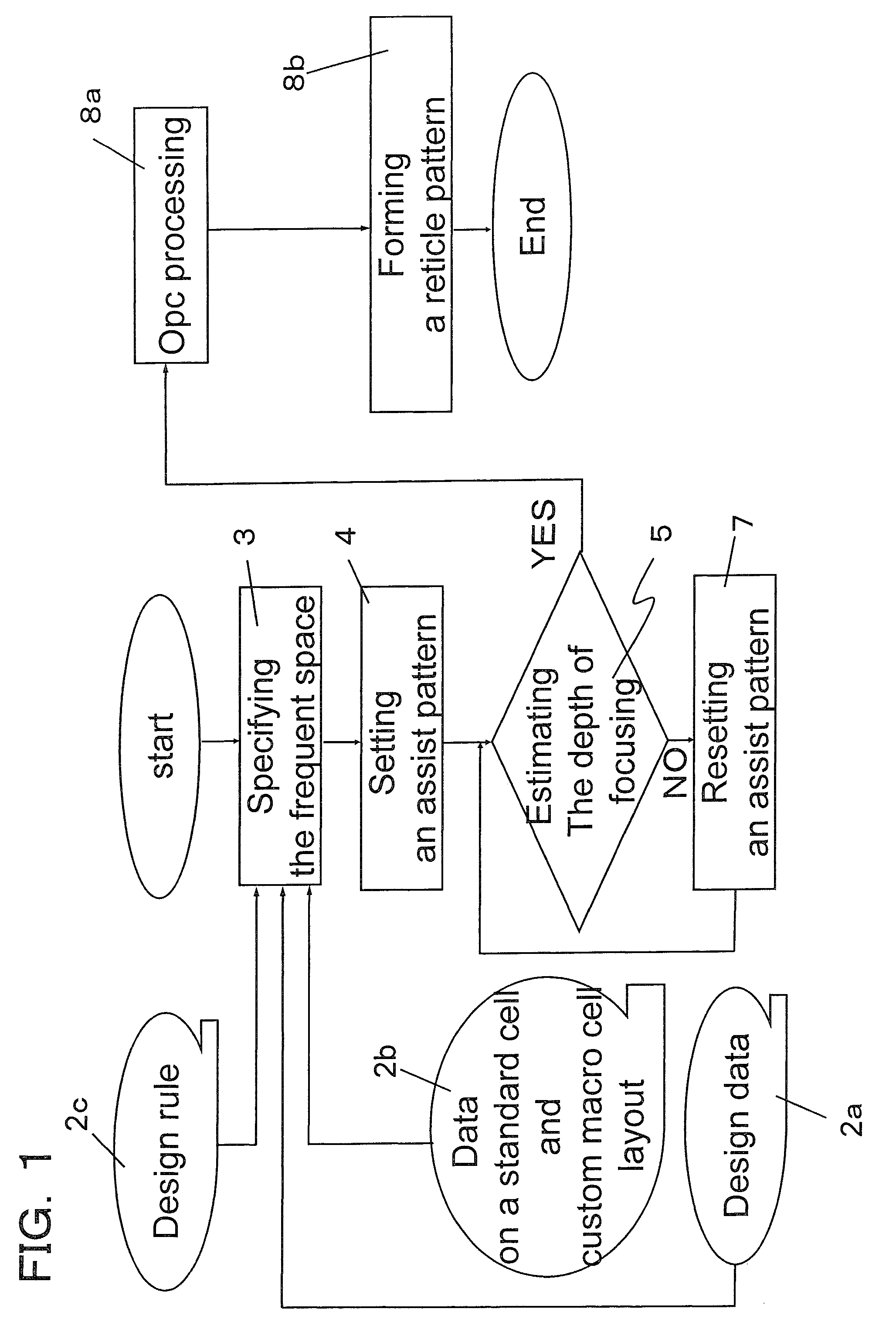
[0026]FIG. 1 is a flowchart showing steps of a reticle manufacturing method according to the first embodiment. Referring to FIG. 1, ...

second embodiment

2. Second Embodiment

[0104]A description will be given of a reticle manufacturing method according to the second embodiment with reference to FIG. 9. Herein, a reticle according to the second embodiment is for forming a contact pattern of the semiconductor apparatus. Further, similarly to the manufacturing method of the photomask according to the first embodiment, the method for manufacturing the reticle for forming the contact pattern according to the second embodiment includes the steps shown in the flowchart in FIG. 1.

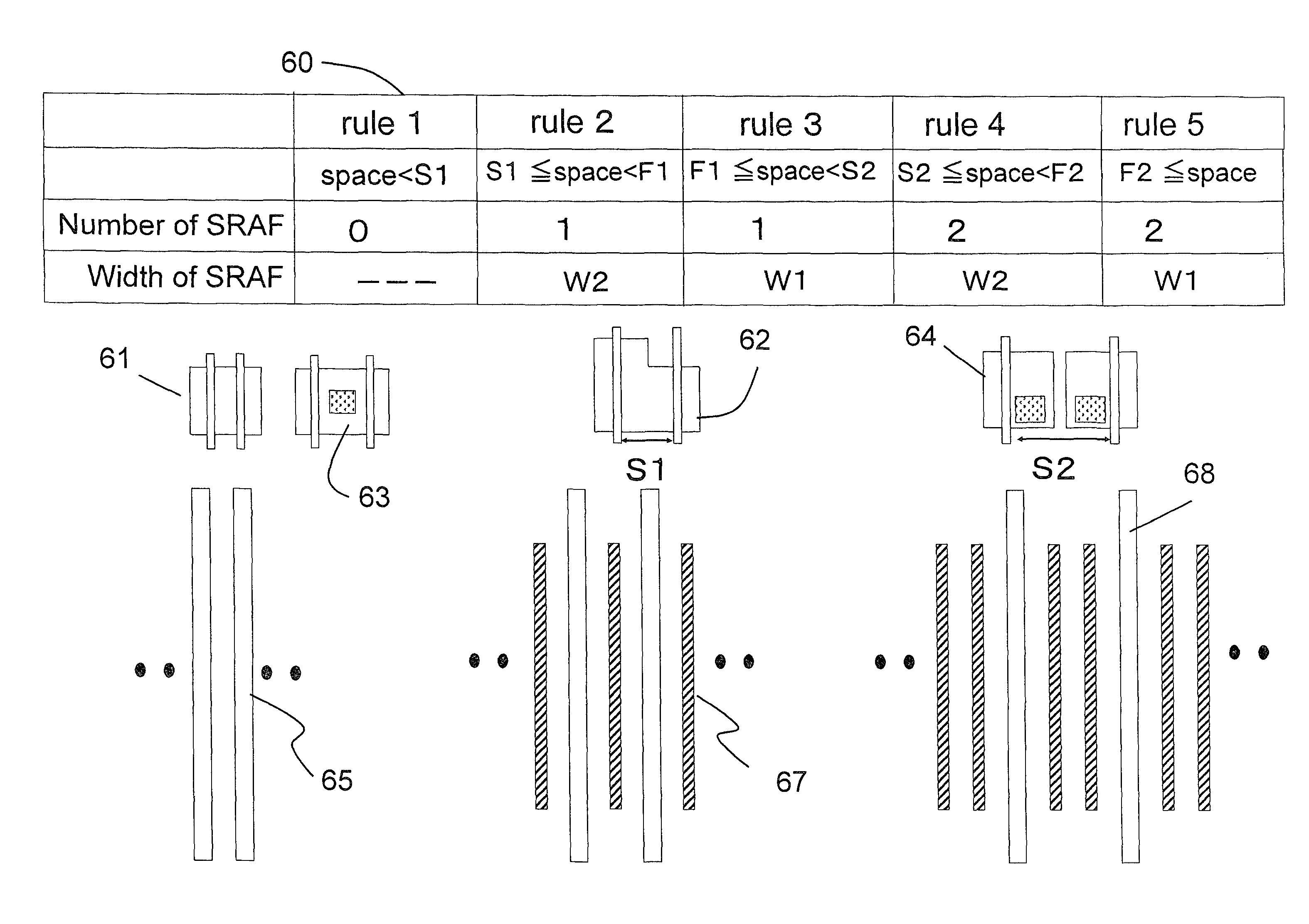
[0105]However, unlike the first embodiment, the main pattern of the reticle manufactured in the flowchart shown in FIG. 1 is based on the contact pattern of the semiconductor apparatus. Therefore, the frequent space is different among the spaces between the main patterns. Further, the assist pattern is arranged to ensure the necessary depth of focus for the formed image of the main pattern having the frequent space following the different rules.

[0106]Incidentally, th...

third embodiment

3. Third Embodiment

[0119]A description will be given of a reticle manufacturing method according to the third embodiment with reference to FIG. 10. Herein, a reticle according to the third embodiment is for forming a wiring pattern of the semiconductor apparatus. Further, the method for the reticle to form the wiring pattern according to the third embodiment includes the steps shown in the flowchart in FIG. 1, similarly to the reticle manufacturing method according to the first embodiment.

[0120]However, unlike the first embodiment, the main pattern of the reticle manufactured in the flowchart shown in FIG. 1 is based on the wiring pattern of the semiconductor apparatus. Therefore, among the spaces between the main patterns, the frequent space is different. Further, the arrangement of the assist pattern for ensuring a necessary depth of focus for the formed image of the main pattern having the frequent space is also different.

[0121]FIG. 10 is a diagram for illustrating the reticle ma...


PUM

PropertyMeasurementUnit
wavelengthaaaaaaaaaa
depth of focusaaaaaaaaaa
depths of focusaaaaaaaaaa

Abstract

A method for creating a pattern on a photomask includes steps of recognizing a space between main patterns by using pattern data which indicate the main patterns to be adjacently transferred onto a wafer, determining a 1st rule about arrangement of an assist pattern on the photomask, the assist pattern being adjacent to the main patterns and not being transferred onto the wafer, estimating a depth of focus in the presence of the assist pattern among the main patterns, determining a 2nd rule about arrangement of the assist pattern on the photomask to improve the depth of focus in the presence of the 1st assist pattern among the main patterns in a group having one or more number of appearance times of the space between main patterns, and correcting the assist pattern on the photomask using the assist pattern data on the basis of the 2nd rule.

Description

BACKGROUND OF THE INVENTION[0001]1. Field of the Invention[0002]The present invention relates to a manufacturing method of a photomask that is preferable to the miniaturization of a pattern of a semiconductor apparatus and a manufacturing method of a semiconductor apparatus using the photomask. In particular, the present invention relates to a manufacturing method of a photomask that optimizes a sub resolution assist feature on a photomask so as to ensure the depth of focus for a formed image of a pattern for circuit formation of the photomask and a manufacturing method of a semiconductor apparatus using the photomask.[0003]2. Description of the Related Art[0004]In accordance with the miniaturization of the device size of a semiconductor apparatus, a resist pattern created by exposure from a photomask pattern is a pattern of approximately half of a wavelength of illumination light used for the exposure, i.e., a sub wavelength pattern in a photo-lithography step serving as one of man...

Claims


Application Information

Patent Timeline
Patent Type & Authority Patents(United States)
IPC IPC(8): G06F17/50G03C5/00G03F1/00G03F1/36G03F1/68G03F1/70H01L21/82
CPCG03F1/144H01L27/0207G03F1/36
Inventor OSAWA, MORIMIMINAMI, TAKAYOSHIASAI, SATORU
Owner FUJITSU SEMICON LTD
Why Eureka
Try Eureka