Distributed interconnect
a distributed interconnect and interconnection technology, applied in the field of interconnections, can solve the problems of limiting the performance of parallel approach and the limited microwave performance of simple paralleling two high inductance interconnects, and achieve the effects of increasing bandwidth, reducing coupling inductance, and increasing the impedance characteristic of the firs
- Summary
- Abstract
- Description
- Claims
- Application Information
AI Technical Summary
Benefits of technology
Problems solved by technology
Method used
Image

Examples
first embodiment
Distributed Interconnect Utilizing a Tapered Trace (First Embodiment)
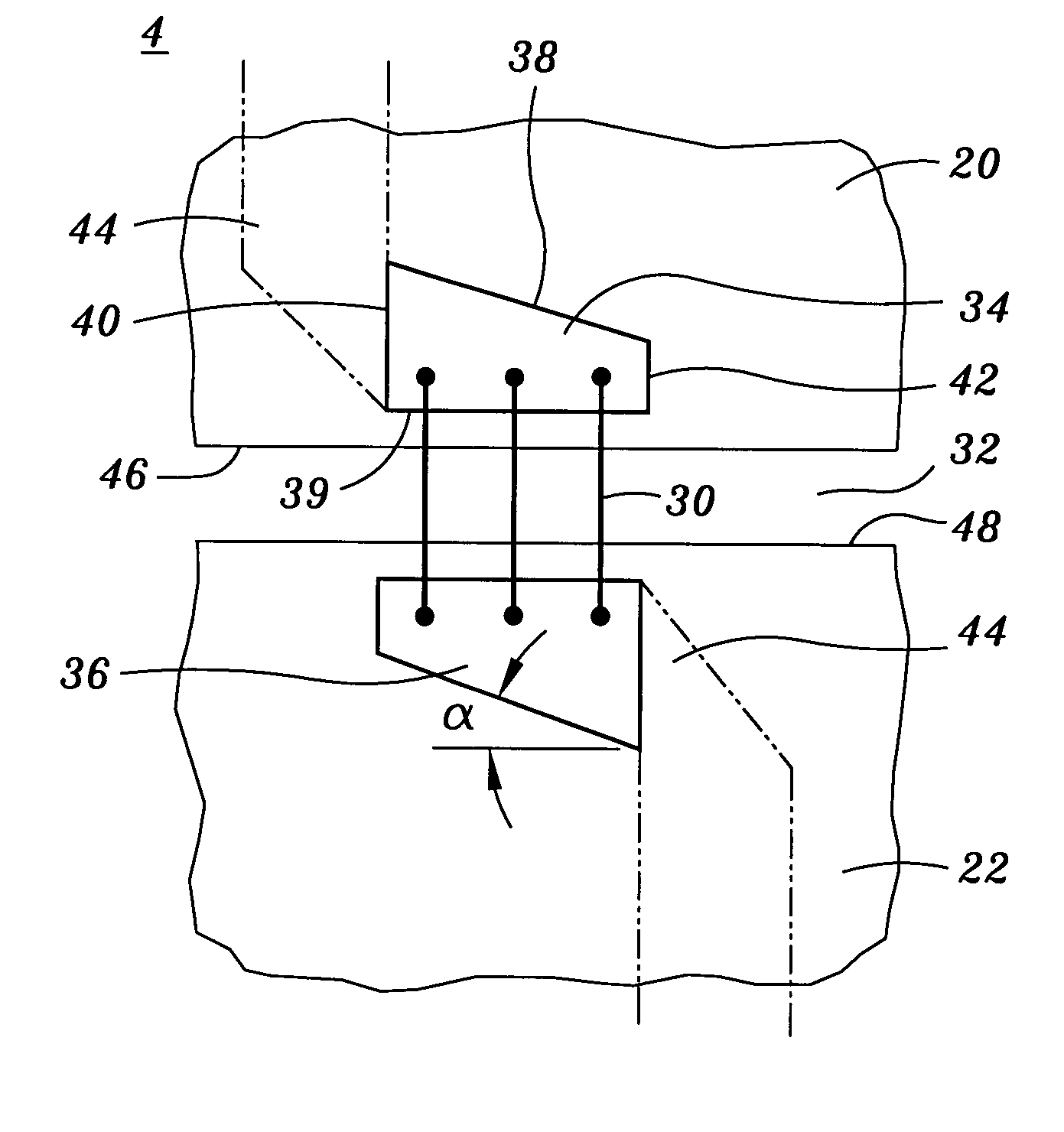
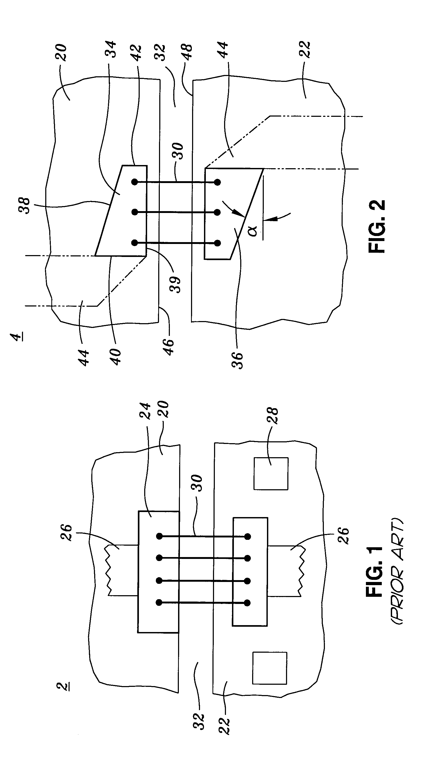
[0042]FIG. 2 is an illustration of a first exemplary embodiment of the present invention which is a distributed interconnect 4 utilizing and a pair of opposing tapered traces 34, 36. The first exemplary embodiment utilizes a first tapered metal trace 34 disposed on the upper surface of a first substrate 20, and a second tapered metal trace 36 disposed on the upper surface of a second substrate 22. The first substrate 20 is provided with a first generally straight edge 46 positioned next to the second substrate 22 having a second generally straight edge 48 such that the first and second substrates 20, 22 form a parallel gap 32 there between. The first trace 34 has a tapered shape. In particular, the first trace 34 has a base side 39 laterally spaced and parallel to said first generally straight edge 46, a short side 42 and tall side 40 oriented normal to said base side 39 and a tapered or inclined side 38 connecting...
second embodiment
Distributed Interconnect Utilizing a Stepped Trace (Second Embodiment)
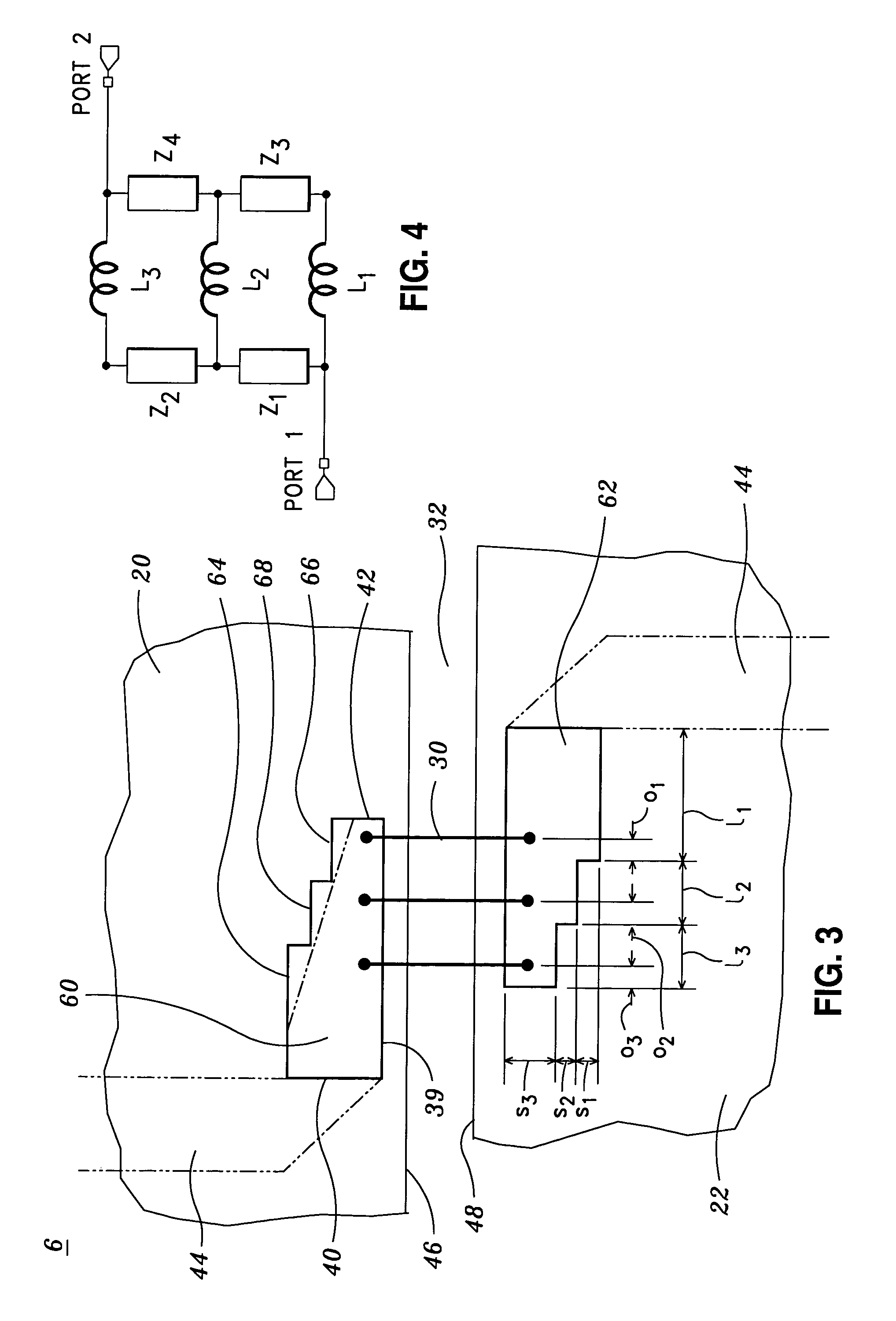
[0043]FIG. 3 is an illustration of a second exemplary embodiment of the present invention which is a distributed interconnect 6 utilizes a pair of opposing stepped traces 60, 62. The first stepped trace 60 is disposed on the upper surface of a first substrate 20 and the second tapered trace 62 is disposed on the upper surface of a second substrate 22. The first substrate 20 is provided with a first generally straight edge 46 positioned next to the second substrate 22 having a second generally straight edge 48 such that the first and second substrates 20, 22 form a parallel gap 32 there between. The first trace 60 has a stepped shape. In particular, the first trace 60 has a base side 39 laterally spaced and parallel to said first generally straight edge 46, a short side 42 and tall side 40 oriented normal to said base side 39 and a stepped side 64 with downwardly proceeding steps connecting the short and tall side ...
embodiments
Model of First and Second Exemplary Embodiments
[0044]FIG. 4 is an electrical schematic which models the first and second exemplary embodiments shown in FIGS. 2 and 3, according to an aspect of the present invention. In particular, the first and second embodiment of the distributed interconnect device 4, 6 may be modeled as having a transmission line with characteristic impedances Z1, Z2, Z3 and Z4 with respective electrical lengths. It is noted that Z2>Z1 and Z3>Z4, which simulates the “tapered” or “stepped” transmission line feature. Inductances L1, L2 and L3, which simulate the bondwires having equal inductive characteristics (i.e., L1=L2=L3), are distributed along the transmission line. As a result of the following transmission line circuit, inductances L1, L2 and L3 are far enough apart to minimize mutual inductance. Ports 1 and 2 are considered the input / output ports of the device 4, 6.
PUM
 Abstract
Description
Claims
Application Information
 - R&D Engineer
- R&D Manager
- IP Professional
- Industry Leading Data Capabilities
- Powerful AI technology
- Patent DNA Extraction
Browse by: Latest US Patents, China's latest patents, Technical Efficacy Thesaurus, Application Domain, Technology Topic.
© 2024 PatSnap. All rights reserved.Legal|Privacy policy|Modern Slavery Act Transparency Statement|Sitemap