

Coating and developing system and coating and developing method with antireflection film and an auxiliary block for inspection and cleaning
a technology of developing system and developing method, which is applied in the direction of basic electric elements, instruments, printing, etc., can solve the problems of large processing block, large area, and inability to produce carrying programs for each of the desired resist films, so as to reduce the need for space and simplify the software
- Summary
- Abstract
- Description
- Claims
- Application Information
AI Technical Summary
Benefits of technology
Problems solved by technology
Method used
Image

Examples
Embodiment Construction
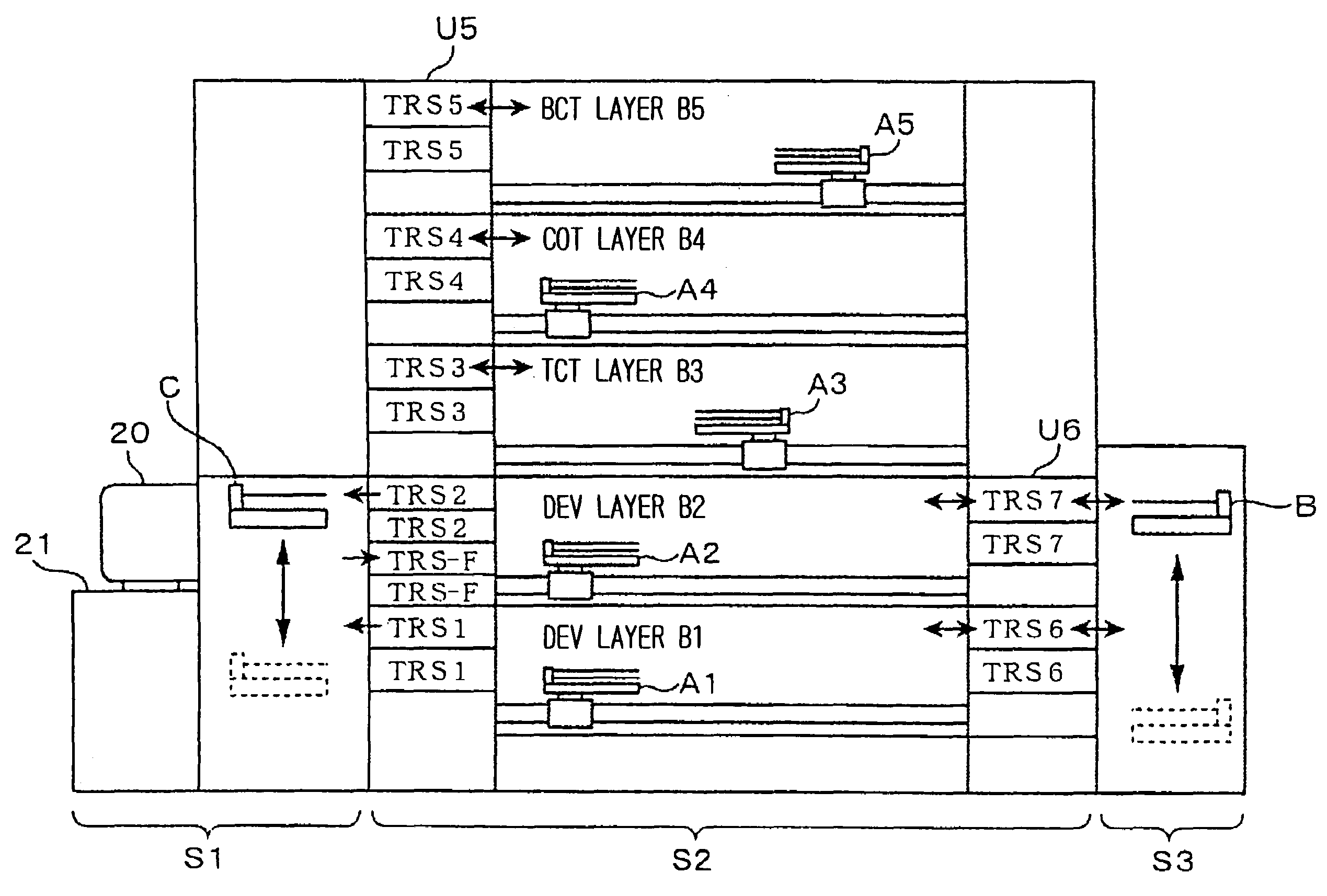
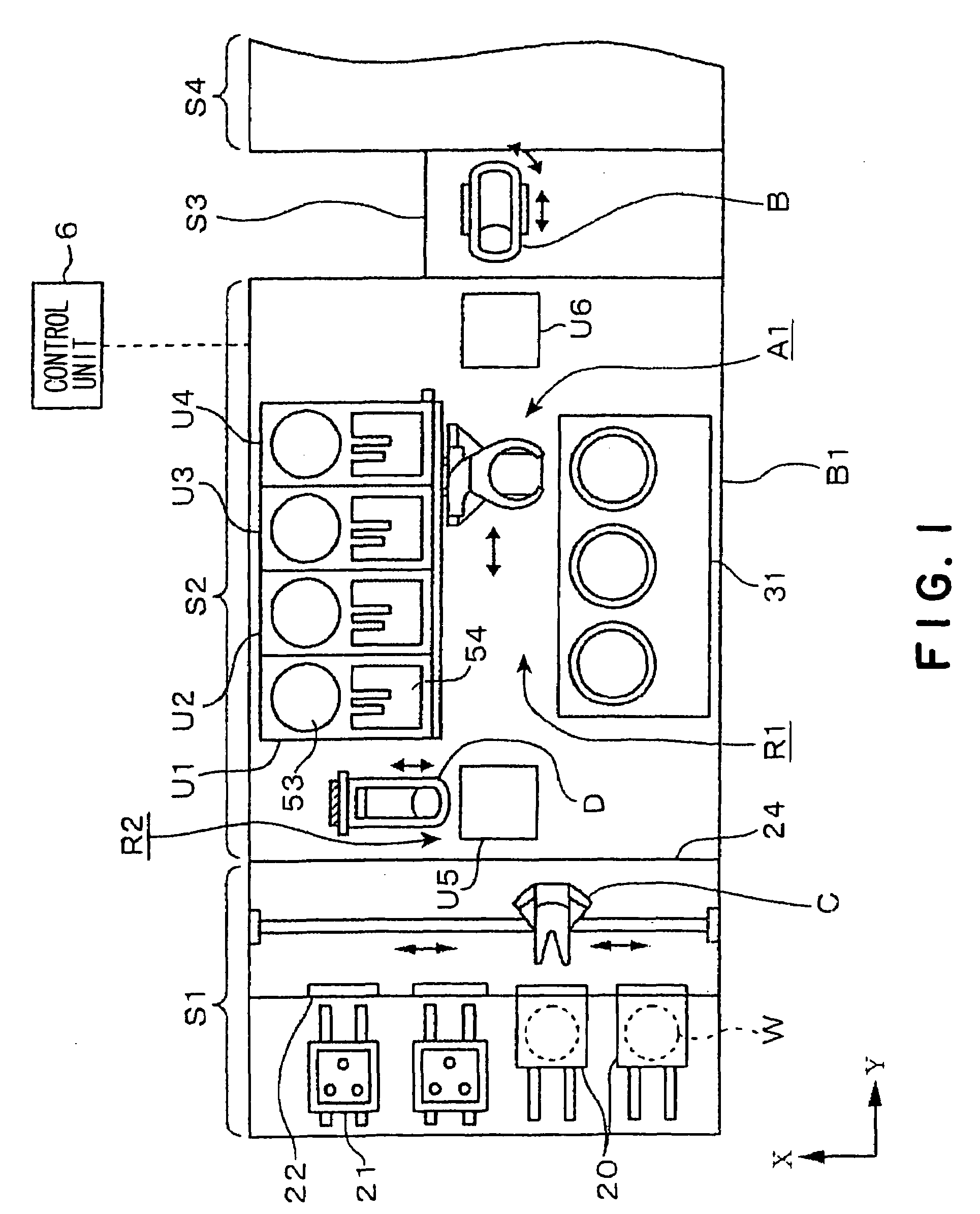
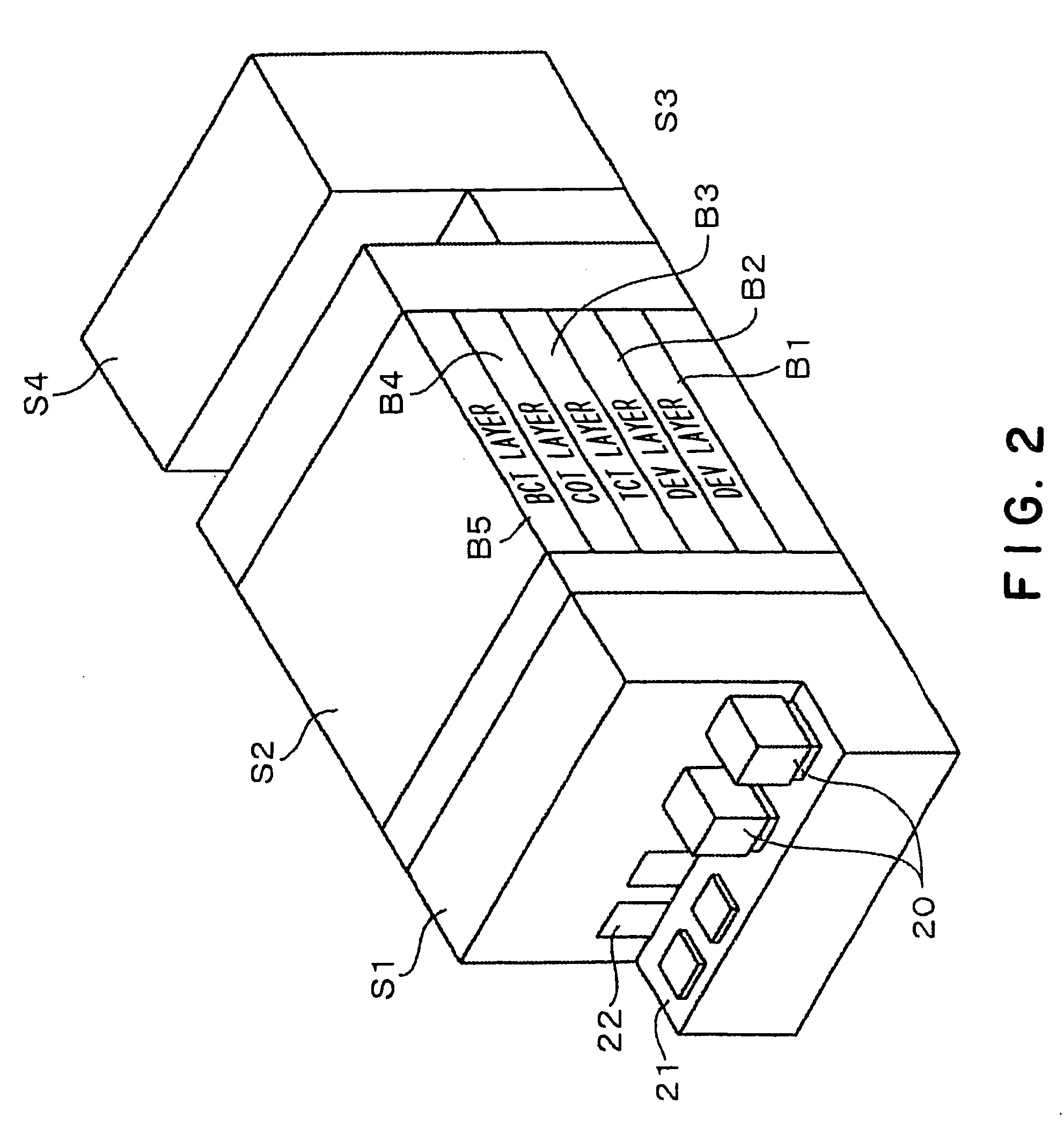
[0039]A coating and developing system in a first embodiment according to the present invention will be described. FIG. 1 is a schematic plan view of a coating and developing system in a first embodiment according to the present invention to be used as a resist pattern forming system, FIG. 2 is a schematic perspective view of the coating and developing system and FIG. 3 is a schematic sectional side elevation of the coating and developing system. The coating and developing system has a carrier handling block S1 for receiving a closed carrier 20 holding, for example, thirteen wafers W, namely, substrates, and sending the same out, a processing block S2 including, for example, five vertically arranged unit blocks B1 to B5, and an interface block S3. An exposure system S4 is connected to the interface block S3.
[0040]The carrier handling block S1 has a carrier support table 21 capable of supporting a plurality of carriers 20 thereon, gates 22 formed in a wall behind the carrier support t...
PUM
 Abstract
Description
Claims
Application Information