
Solid-state image pickup device, optical apparatus, signal processing apparatus, and signal processing system

Inactive Publication Date: 2010-04-15
SONY CORP
View PDF17 Cites 10 Cited by
  • Summary
  • Abstract
  • Description
  • Claims
  • Application Information

AI Technical Summary

Benefits of technology

[0016]According to the present invention, since the solid-state image pickup device is provided with a light modulation unit that modulates an externally input light beam using a pixel signal read from the pixel unit, the solid-state image pickup device can output a signal through optical communication without including a light emitting element. In addition, by synchronizing the input and output of the signal with a synchronization signal, the solid-state image pickup device can convert an electrical signal photoelectrically converted from light input to the pixel unit into an optical signal and output the optical signal. In this way, generation of heat caused by optical communication can be prevented and, therefore, a negative impact of heat on the pixel unit can be reduced. In addition, power consumption for the optical communication can be reduced.
[0017]Since a negative impact of heat can be reduced, a signal read from the solid-state image pickup device can be transmitted at high speed. In addition, by integrating the elements into one chip, the space necessary for mounting the solid-state image pickup device can be reduced. Furthermore, the design process of the solid-state image pickup device can be facilitated. Since the length of the transmission path of an electrical signal can be reduced, high-speed transmission can be easily achieved.
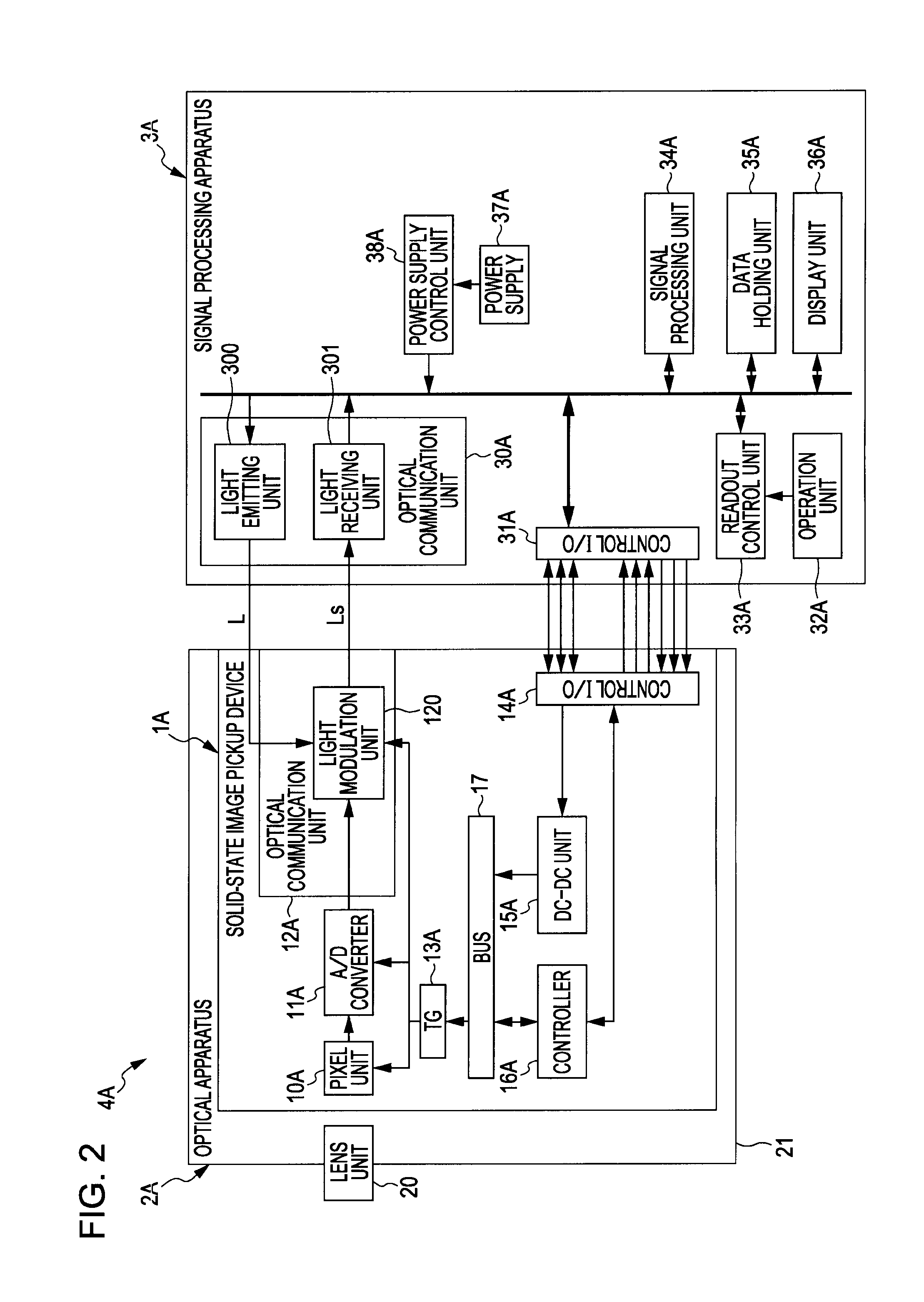
[0018]According to the present invention, the optical apparatus includes the above-described solid-state image pickup device. Therefore, an image of light captured by the solid-state image pickup device can be transmitted at high speed. In addition, according to the present invention, the signal processing apparatus to which the above-described optical apparatus is connected is provided. Therefore, an image of light captured by the solid-state image pickup device can be input to the signal processing apparatus at high speed. As a result, the signal processing apparatus can acquire a large amount of data.
[0019]According to the present invention, the signal processing system includes the above-described optical apparatus and the signal processing apparatus. Therefore, an image of light captured by the solid-state image pickup device can be transmitted at high speed. As a result, the signal processing system can process a large amount of transmission data even when the number of pixels of the solid-state image pickup device or the frame rate is increased.

Problems solved by technology

Accordingly, the image pickup device may receive a negative impact from heat generated by the light emitting element.

Method used


Image

  • Solid-state image pickup device, optical apparatus, signal processing apparatus, and signal processing system
  • Solid-state image pickup device, optical apparatus, signal processing apparatus, and signal processing system
  • Solid-state image pickup device, optical apparatus, signal processing apparatus, and signal processing system

Examples


first embodiment

Outline of Solid-State Image Pickup Device of First Embodiment

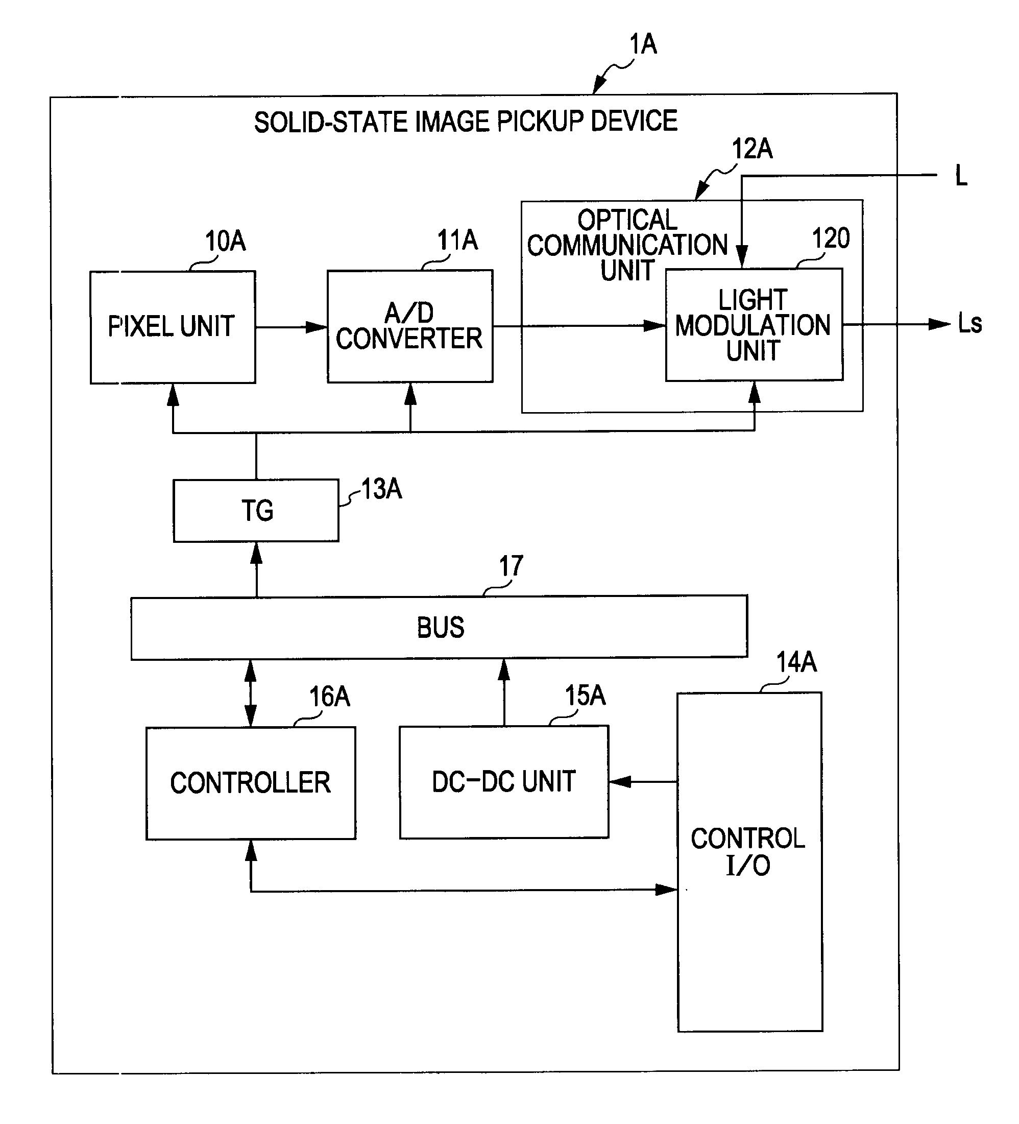
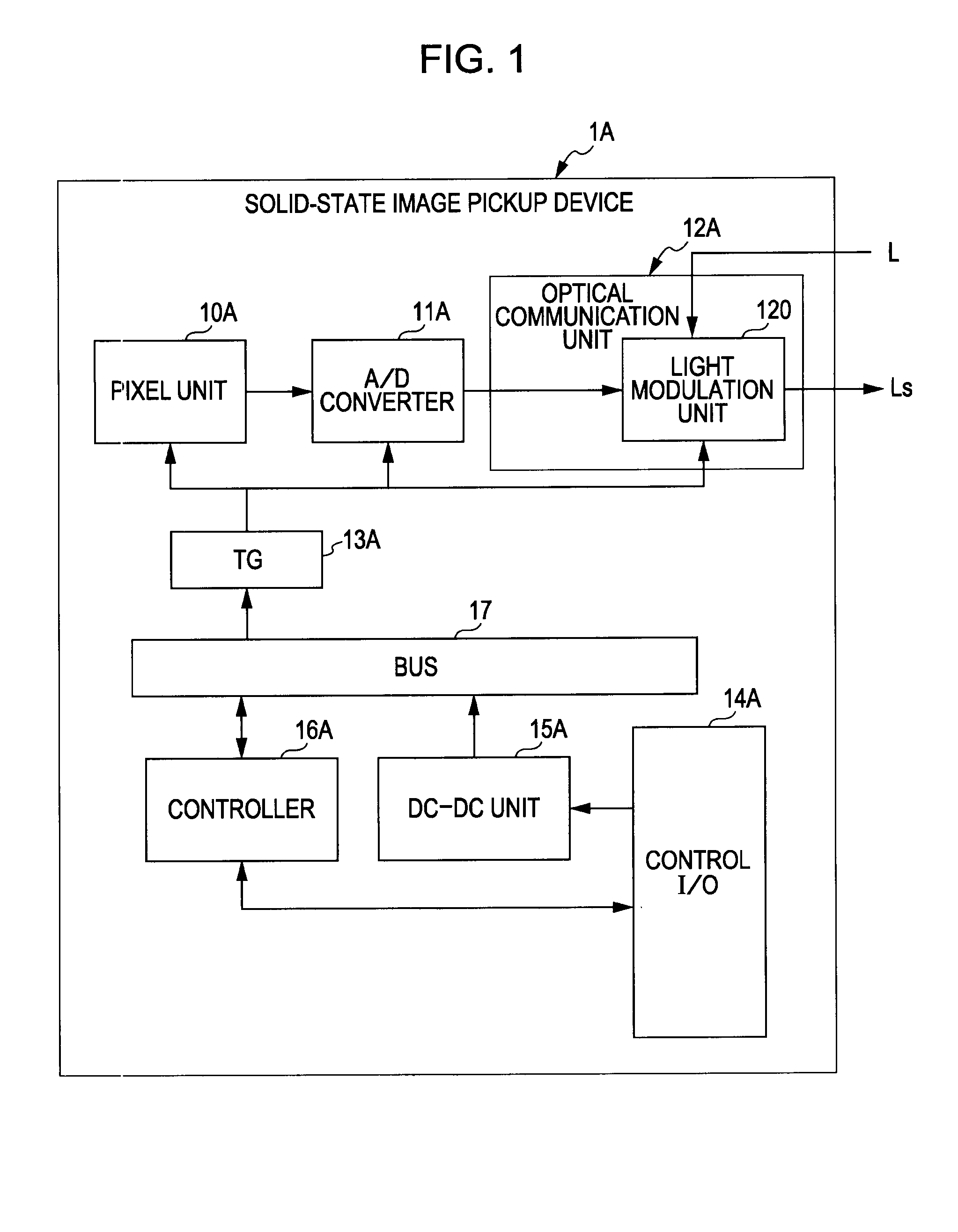
[0066]FIG. 1 is a functional block diagram of a solid-state image pickup device according to a first embodiment of the present invention. According to the present embodiment, a solid-state image pickup device 1A is formed from a complementary metal oxide semiconductor (CMOS) image sensor or a charge coupled device (CCD) image sensor. The solid-state image pickup device 1A includes a pixel unit 10A that converts a light beam into an electrical signal and outputs the electrical signal and an A / D converter 11A that converts the electrical signal output from the pixel unit 10A into a digital signal. The pixel unit 10A includes pixels arranged two-dimensionally or one-dimensionally. The pixels convert light into electrical signals. The pixel unit 10A outputs an electrical signal in accordance with the intensity of incident light.

[0067]The solid-state image pickup device 1A includes an optical communication unit 12A. The optica...

application example

of Signal Processing System

[0248]FIGS. 43 to 45 are functional block diagrams illustrating application examples of the signal processing system according to the first embodiment. In FIG. 43, a ranging apparatus 401B serving as the signal processing system is illustrated. The ranging apparatus 401B includes an optical apparatus 20A. The optical apparatus 20A includes a light emitting unit 410, a light emission control unit 411, and a data comparison operator unit 412. In addition, the signal processing apparatus 3A includes a distance data computing unit 413.

[0249]In the ranging apparatus 401B, the light emitting unit 410 emits light to an object to be distance-measured. The reflected light from the object is made incident on the pixel unit 10A. A phase change in accordance with a distance change is computed by the data comparison operator unit 412 using an electrical signal read from the pixel unit 10A. The computation result of the data comparison operator unit 412 is transmitted f...


PUM


Abstract

A solid-state image pickup device includes a pixel unit configured to convert light into an electrical signal, an A / D converter configured to convert a signal read from the pixel unit into a digital signal, a light modulation unit configured to modulate an externally input light beam using the signal digitized by the A / D converter and output a signal light beam based on the signal read from the pixel unit, a timing generation unit configured to generate a synchronization signal used for synchronizing input and output of signals of the pixel unit, the A / D converter, and the light modulation unit, and a controller configured to control readout of the signal.

Description

BACKGROUND OF THE INVENTION[0001]1. Field of the Invention[0002]The present invention relates to a solid-state image pickup device, an optical apparatus including the solid-state image pickup device, a signal processing apparatus to which the optical apparatus is connected, and a signal processing system including the optical apparatus and the signal processing apparatus. In particular, the present invention relates to a solid-state image pickup device, an optical apparatus, a signal processing apparatus, and a signal processing system capable of modulating an externally input light beam using a pixel signal read from the solid-state image pickup device and outputting a modulated light signal.[0003]2. Description of the Related Art[0004]As the processing speed and the packaging density of circuit boards have increased, problems of a signal delay and the occurrence of EMI (electromagnetic interference) have arisen. Accordingly, optical interconnection technology that solves signal de...

Claims


Application Information

Patent Timeline
IPC IPC(8): H04N5/335H01L27/146H04N5/372H04N5/374H04N5/378
CPCH04N5/378H04N5/23203H04N23/66H04N25/78H04N25/75
Inventor OGASAWARA, HIDEHIKOSEKIYA, TOSHIYUKI
Owner SONY CORP
Learn More