
Electronic device with integral connectors

a technology of integrated connectors and electronic devices, applied in the direction of coupling device connections, coupling protective earth/shielding arrangements, printed circuit aspects, etc., can solve the problems of increasing the size of the electronic device containing the pcb, and the size of conventional connectors may be a limiting factor in the attempt to miniaturize portable electronic devices, etc., to achieve the effect of less manufacturing cos

Inactive Publication Date: 2007-07-24
GOOGLE LLC
View PDF12 Cites 43 Cited by
  • Summary
  • Abstract
  • Description
  • Claims
  • Application Information

AI Technical Summary

Benefits of technology

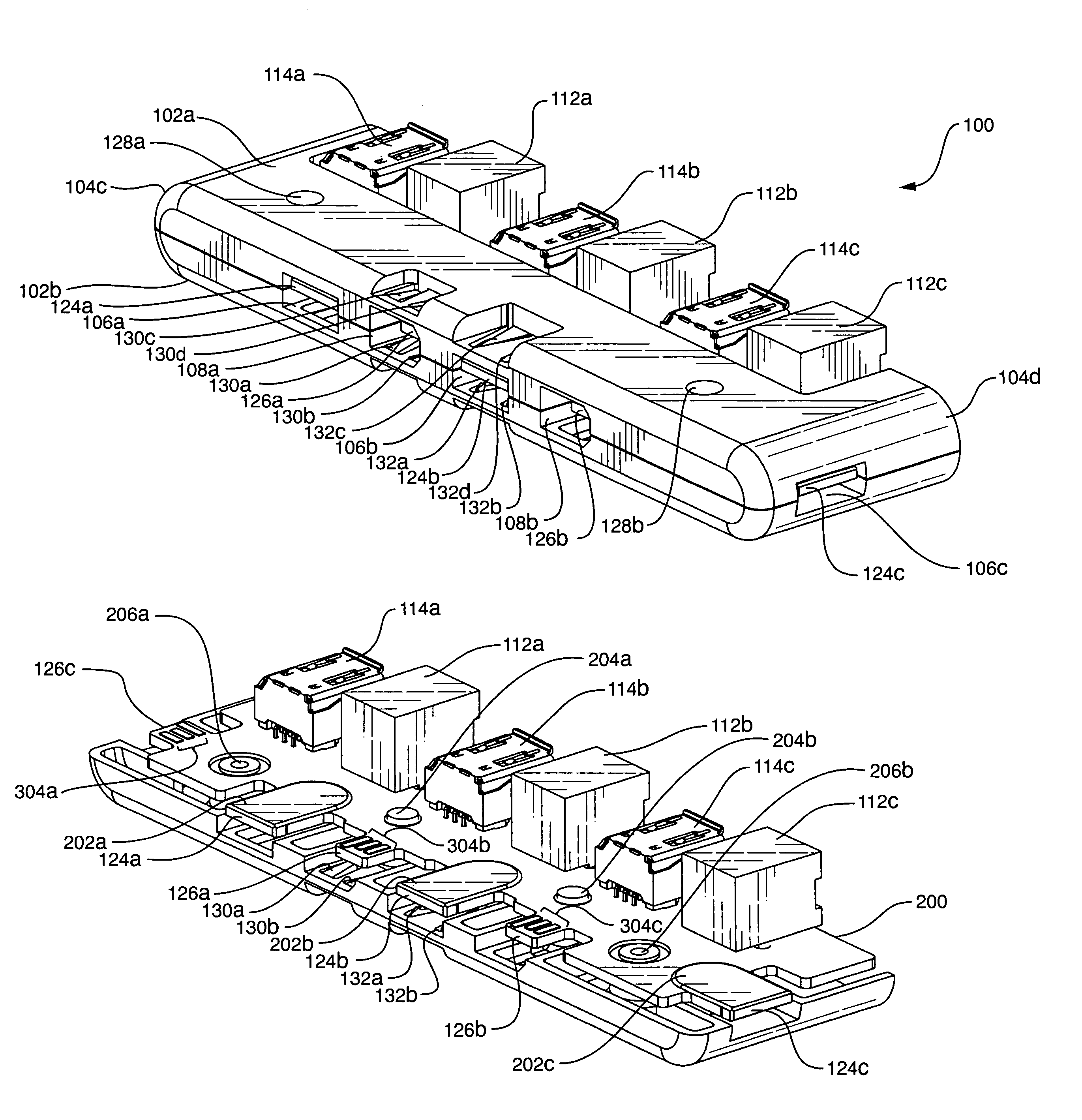
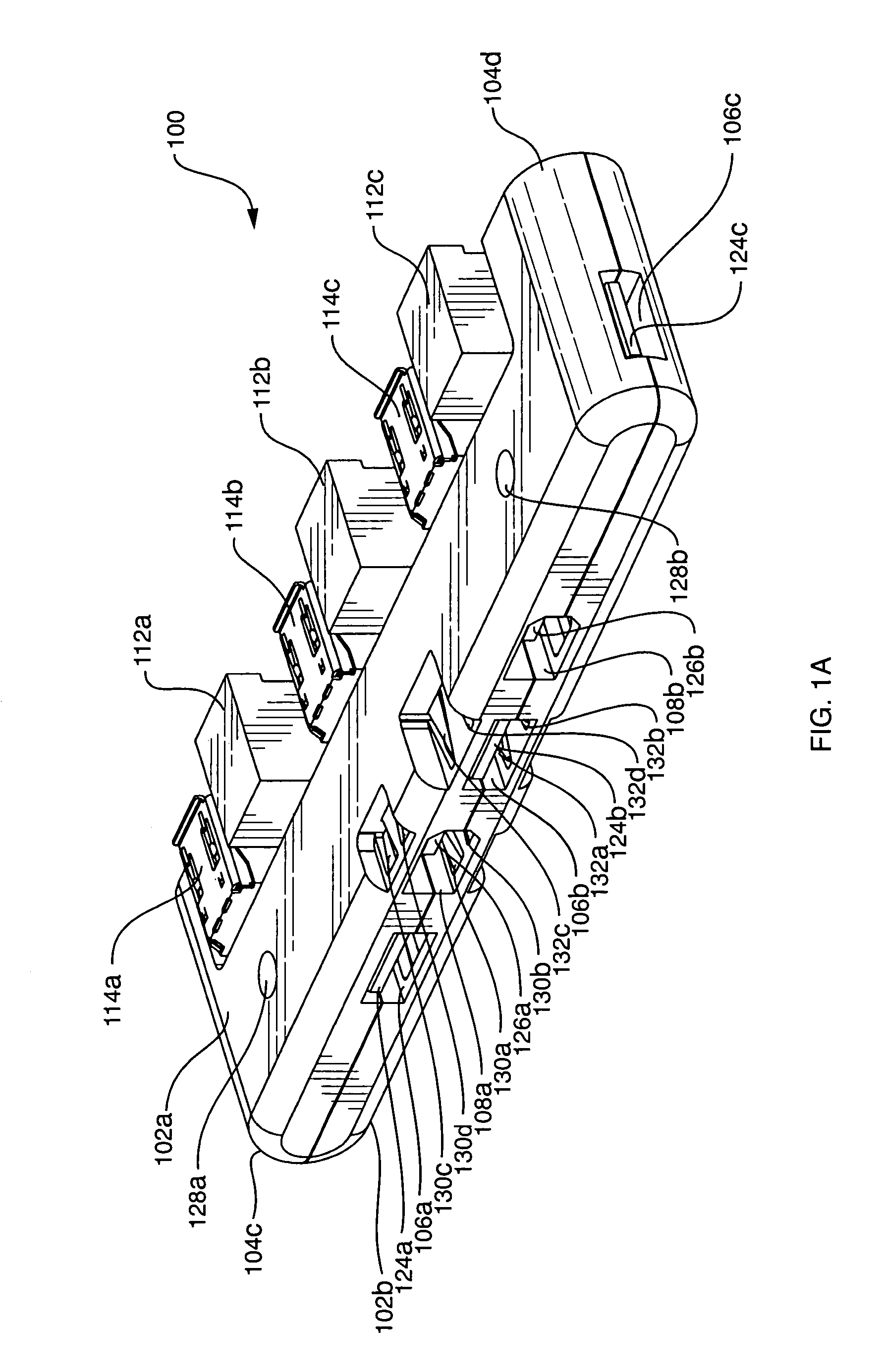
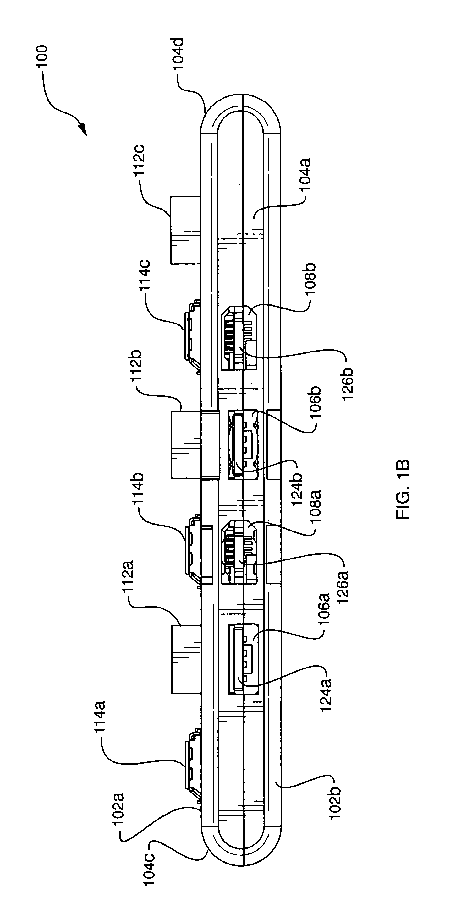
[0010]An electronic device having one or more integral connectors is disclosed. The connector includes an electromagnetically-shielded cavity defined by an outer shell integrally formed in the housing and having a cross-sectional profile of a plug to which the connector may mate. The connector also includes a tongue integrally formed in and extending from a component (such as a printed circuit board) of the electronic device and protruding into the cavity. The tongue may have one or more electrical contacts on one or both sides. The connector may also include one or more snap features for retaining a mated plug at a predetermined force. The connectors may conform to one or more connector standards, such as the Universal Serial Bus (USB) standard and / or the IEEE 1394 (FireWire®) standard. Devices incorporating such integral connectors may be smaller and manufactured less expensively than devices having conventional, non-integral, connectors.

Problems solved by technology

Not all connectors, however, perform all of these functions.
Mounting a conventional connector to a PCB increases the size of the PCB and may thereby increase the size of the electronic device containing the PCB.
The size of conventional connectors may therefore be a limiting factor in attempts to miniaturize portable electronic devices.

Method used


Image

  • Electronic device with integral connectors
  • Electronic device with integral connectors
  • Electronic device with integral connectors

Examples


Embodiment Construction

[0026]In one aspect of the present invention, an electronic device having at least one integral connector is provided. Physical and electrical features of the connectors are integrated into the housing and circuit board of the electronic device itself, thereby eliminating the need for separate connectors. The electronic device's integral connectors may satisfy the requirements of standards such as USB and IEEE 1394 without the use of the distinct connector components that are typically used to implement connectors according to such standards. Furthermore, if multiple connector types in the electronic device share a common physical attribute, such as a central tongue with electrical contacts formed thereon, the same component in the device (e.g., the PCB) may be used to implement the common physical attribute for the multiple connector types.

[0027]In one aspect of the present invention, a connector in an electronic device may be formed from:[0028](1) an electromagnetically-shielded c...


PUM


Abstract

An electronic device having one or more integral connectors is disclosed. The connector includes an electromagnetically-shielded cavity defined by an outer shell integrally formed in the housing and having a cross-sectional profile of a plug to which the connector may mate. The connector also includes a tongue integrally formed in and extending from a component (such as a printed circuit board) of the electronic device and protruding into the cavity. The tongue may have one or more electrical contacts on one or both sides. The connector may also include one or more snap features for retaining a mated plug at a predetermined force. The connectors may conform to one or more connector standards, such as the Universal Serial Bus (USB) standard and / or the IEEE 1394 (FireWire®) standard. Devices incorporating such integral connectors may be smaller and manufactured less expensively than devices having conventional, non-integral, connectors.

Description

CROSS-REFERENCE TO RELATED APPLICATIONS[0001]This application is a divisional application of commonly-owned U.S. patent application Ser. No. 10 / 197,378, filed on Jul. 17, 2002, entitled “Electronic Device with Integral Connectors”.BACKGROUND[0002]1. Field of the Invention[0003]The present invention relates to electronic devices and, more particularly, to connectors for physically and electrically connecting electronic devices to each other.[0004]2. Related Art[0005]Electronic devices, such as personal computers, personal digital assistants (PDAs), and cellular telephones typically have electrical input and output connectors for receiving and transmitting electrical signals. Examples of such connectors include power jacks, headphone jacks, Universal Serial Bus (USB) connectors, IEEE 1394 (FireWire®) connectors, and other connectors which carry data and power into and from electronic devices.[0006]Typically, a plug at the end of a cable is connected to a device connector, thereby form...

Claims


Application Information

Patent Timeline
Patent Type & Authority Patents(United States)
IPC IPC(8): H01R12/00H01R13/658H01R13/66H01R27/02H05K1/11
CPCH01R13/6658H01R27/00H01R27/02H05K1/117H01R13/659H01R23/6873H05K2201/09145H05K2201/10325H01R12/721
Inventor MERZ, NICHOLAS G. L.
Owner GOOGLE LLC
Learn More