Wiring board, semiconductor device and display module

a technology of display modules and wiring boards, applied in the field of wiring boards, can solve the problems of easy cracks and ruptures of conductive wirings, and the folding resistance of conductive wirings made of copper leads cannot be sufficient anymore, so as to suppress the occurrence of wiring breakage

Inactive Publication Date: 2007-07-31
PANASONIC CORP
View PDF11 Cites 31 Cited by
  • Summary
  • Abstract
  • Description
  • Claims
  • Application Information

AI Technical Summary

Benefits of technology

[0010]Therefore, with the foregoing in mind, it is an object of the present invention to provide a wiring board where bending stress applied to the conductive wirings is relieved sufficiently even when the thickness of the film base or the like is reduced, so that the occurrence of breaks in the wirings can be suppressed.

Problems solved by technology

However, in the structure, since the film base is not provided at the folded portion where the slit is formed, mechanical stress during the packaging or stress caused by a heat cycle or the like will be concentrated to the conductive wirings made of a thin copper lead, and cracks and ruptures in the conductive wirings can occur easily.
However, even in the wiring board having the above-mentioned conventional structure, folding resistance of the conductive wirings made of a copper lead cannot be sufficient anymore.

Method used


Image

  • Wiring board, semiconductor device and display module
  • Wiring board, semiconductor device and display module
  • Wiring board, semiconductor device and display module

Examples


Embodiment Construction

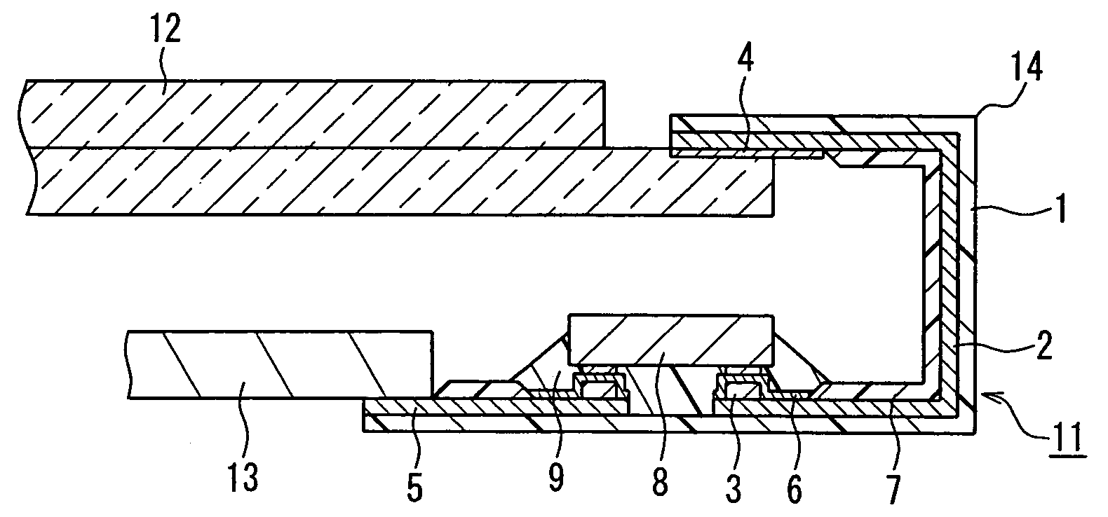
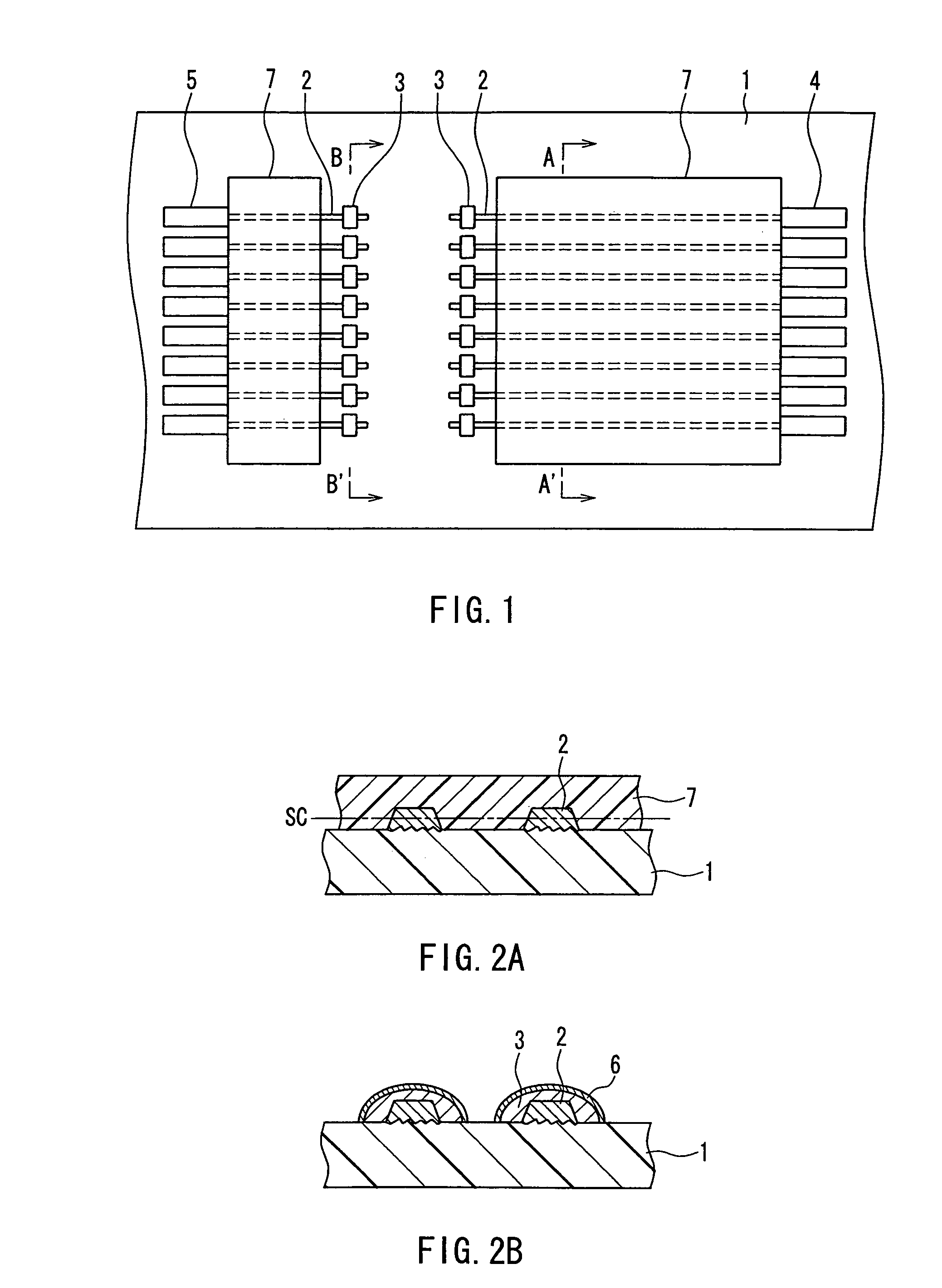
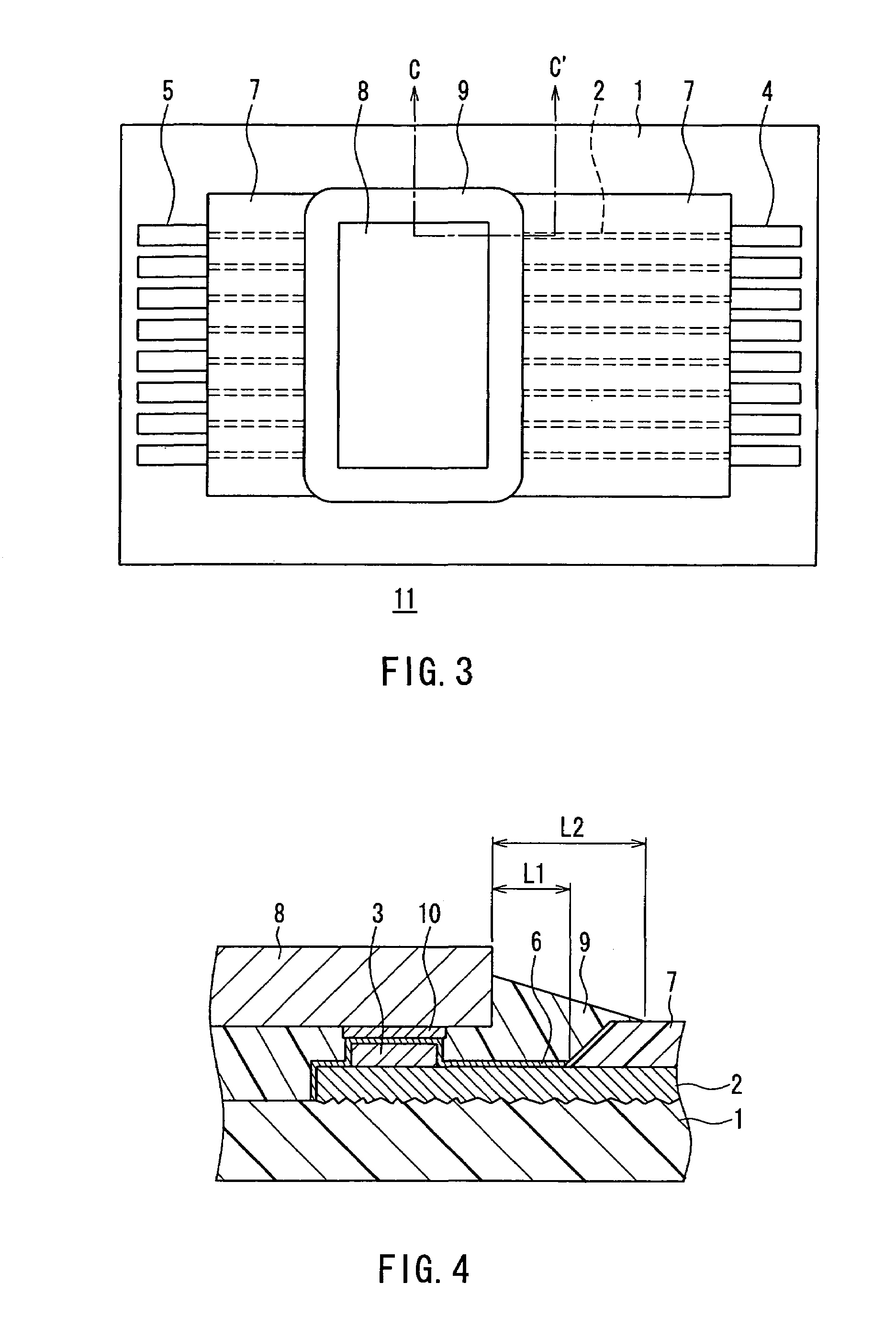
[0020]According to the thus configured wiring board of the present invention, since metal plating layers are not applied on regions where solder resist layers are formed, increase in brittleness of the conductive wirings, which is caused by formation of the metal plating layers, can be avoided. Moreover, by roughening the surfaces of the conductive wirings at the portions to be contacted with the base, adherence between the conductive wirings and the base is increased. Furthermore, due to the structure of sandwiching the conductive wirings between the base and the solder resist layers, the conductive wirings are fixed to the base so as to improve the effect of relieving the bending stress. As a result, by positioning a folding portion in regions where the solder resist layers are formed, occurrence of breaks in the conductive wirings can be suppressed.

[0021]It is preferable in the wiring board of the present invention that the elastic moduli and the thicknesses of the materials for ...


PUM


Abstract

A wiring board includes: a flexible insulating base 1; a plurality of conductive wirings 2 arranged on the flexible insulating base 1; protruding electrodes 3 provided respectively at an end portion of the same side of each of the conductive wirings; external terminals 4, 5 formed respectively at the other end portions of each of the conductive wirings; metal plating layers applied on the conductive wirings, the protruding electrodes and the external terminals; and solder resist layers 7 formed respectively by coating the conductive wirings in regions between the end portions at which the protruding electrodes are provided and the external terminals. In the regions where the solder resist layers are formed, no metal plating layers are formed on the conductive wirings, and the surfaces of the conductive wirings to be contacted with the flexible insulating base are rougher than the surfaces not to be contacted with the flexible insulating base. Even when a film base is thin, bending stress applied to the conductive wirings is relieved sufficiently, and thus breaks in the wirings are suppressed.

Description

BACKGROUND OF THE INVENTION[0001]1. Field of the Invention[0002]The present invention relates to a wiring board such as a tape carrier substrate formed by providing a conductive wiring on a flexible insulating base. Particularly, the present invention relates to a structure of a wiring board having conductive wirings whose folding resistance is improved.[0003]2. Description of Related Art[0004]As one type of package module using a tape carrier substrate, the one employing a COF (Chip On Film) has been known. The COF includes a semiconductor chip mounted on a flexible insulating tape carrier substrate and the mounted portion is protected by sealing with a resin. The tape carrier substrate includes as main components an insulating film base and a plurality of conductive wirings formed on a surface of the film base. In general, polyimide is used as a material of the film base and copper is used as a material of the conductive wirings. As required, a metal plating film and a solder resi...

Claims


Application Information

Patent Timeline
Patent Type & Authority Patents(United States)
IPC IPC(8): H05K3/46
CPCH05K1/028H05K1/111H05K3/243H05K1/189H05K3/025H01L2224/73204H05K3/382H05K3/4007H05K2201/0367H05K2201/10674H05K3/28Y02P70/50
Inventor NAGAO, KOUICHINAKAMURA, YOSHIFUMIIMAMURA, HIROYUKITETANI, MICHINARI
Owner PANASONIC CORP
Why Eureka
Try Eureka