Semiconductor device
a technology of semiconductor devices and semiconductors, applied in semiconductor devices, semiconductor/solid-state device details, electrical apparatus, etc., to achieve the effect of reducing the entrance of light from the lateral direction, reducing the width, and inhibiting the fluctuation of properties
- Summary
- Abstract
- Description
- Claims
- Application Information
AI Technical Summary
Benefits of technology
Problems solved by technology
Method used
Image
Examples
first embodiment
1. First Embodiment
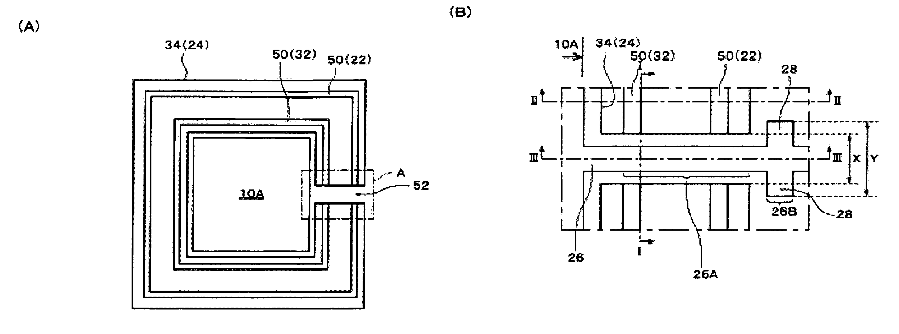
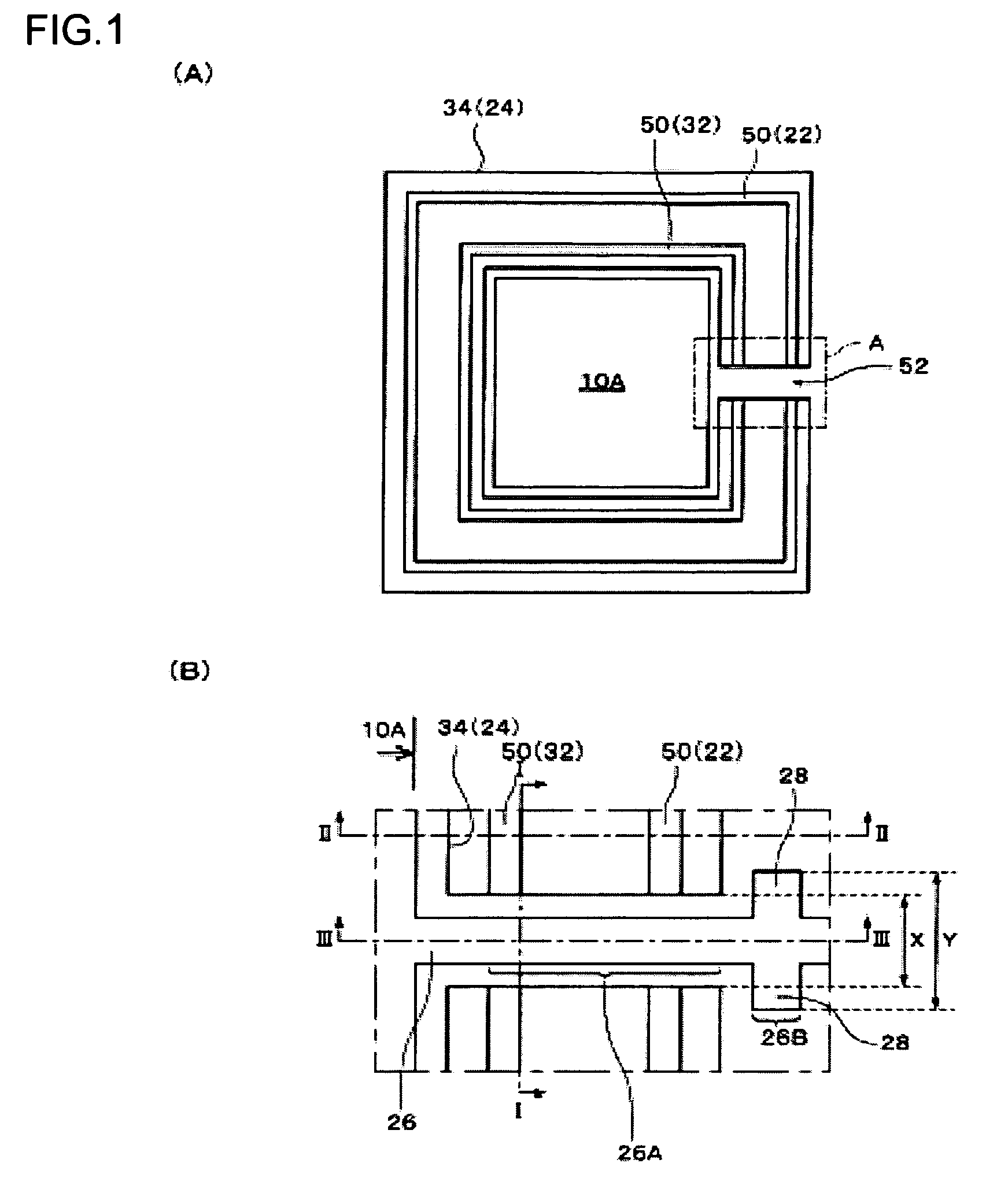
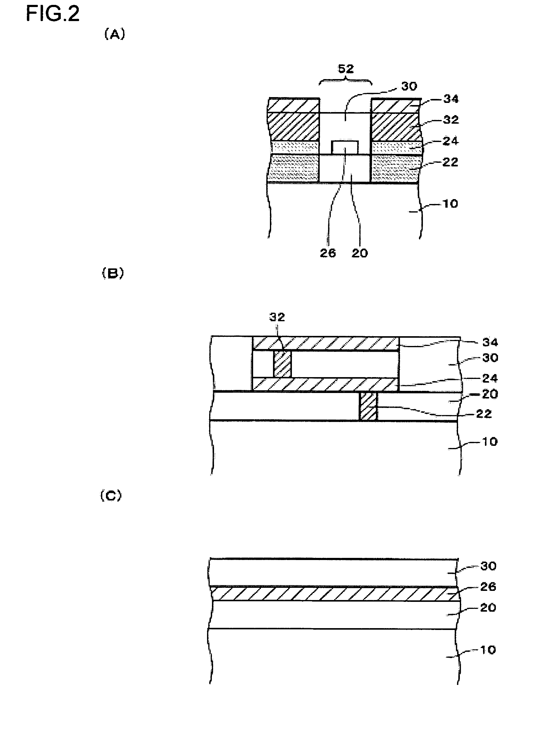
[0034]A semiconductor device of a first embodiment will be described with reference to FIGS. 1 and 2. FIG. 1A is a two-dimensional pattern diagram showing a semiconductor device according to the embodiment. FIG. 1B is an enlarged diagram showing part A in FIG. 1A. FIG. 2A is a sectional view along line I-I in FIG. 1B, FIG. 2B is a sectional view along line II-II, and FIG. 2C is a sectional view along line III-III.
[0035]As shown in FIG. 1A, a semiconductor device according to the embodiment has an element forming area 10A, on which various kinds of semiconductor elements are set up on a semiconductor layer (not shown). Elements, such as a nonvolatile memory having a floating gate electrode (including a memory cell array) and a MOS transistor, the properties of which change in response to light are set up on the element forming area 10A. A light shielding wall 50 is set up around the element forming area 10A. The light shielding wall 50 is set up so that entrance of...
second embodiment
2. Second Embodiment
[0045]Next, a second embodiment will be described with reference to FIGS. 3 to 7. FIGS. 3 and 4 are diagrams showing a nonvolatile memory cell (hereinafter simply referred to as a “memory cell”) that is set up on the element forming area 10A in the semiconductor device according to the second embodiment. FIG. 5 is a two-dimensional pattern diagram showing a semiconductor device according to the second embodiment. FIG. 6A is a sectional view along line I-I in FIG. 5, and FIG. 6B is a sectional view along line II-II in FIG. 5. FIG. 7 is a two-dimensional diagram showing a modification example of semiconductor devices according to the second embodiment.
[0046]First, a memory cell, which is a semiconductor element set up on the element forming area 10A, will be described.
[0047]In a memory cell 120 that is included in the semiconductor device of the embodiment, a control gate is an n-type impurity area within a semiconductor layer 10, and a floating gate electrode is c...
modification example
[0060]Next, a semiconductor device according to a modification example of the second embodiment will be described with reference to FIG. 7. FIG. 7 is a two-dimensional diagram showing a semiconductor device according to a modification example of the second embodiment, showing a plane surface corresponding to FIG. 5.
[0061]In a semiconductor device according to the modification example, the directions in which the signal wires 26 and 27 are drawn out are different from each other, as shown in FIG. 7. Specifically, the holes 52 and 54, or the part where the light shielding wall 50 is not set up, are respectively set up on different edges of the element forming area 10A. The signal wire 26 is drawn out through the hole 52 and the signal wire 27 is drawn out through the hole 54. The signal wires 26 and 27 respectively include a pattern that includes second parts 26B or 27B the widths of which are larger than the widths of the holes 52 and 54. Thus, entrance of light from the lateral dire...
PUM
 Abstract
Description
Claims
Application Information


