Battery mounted integrated circuit device having diffusion layers that prevent cations serving to charge and discharge battery from diffusing into the integrated circuit region

a technology of integrated circuit device and diffusion layer, which is applied in the direction of cell components, secondary cells servicing/maintenance, cell components, etc., can solve the problems of increasing the amount of n-type impurity required, deteriorating or improper operation of semiconductor devices, and increasing the time required for the formation of diffusion layers

Active Publication Date: 2007-08-07
PANASONIC CORP
View PDF12 Cites 48 Cited by
  • Summary
  • Abstract
  • Description
  • Claims
  • Application Information

AI Technical Summary

Problems solved by technology

When those ions having diffused in the semiconductor substrate reach semiconductor devices, there are possibilities that the characteristics of the semiconductor devices deteriorate or the semiconductor devices improperly operate.
This leads to an increase in amount of the N-type impurity required for increasing the concentration of the N-type impurity in the diffusion layer.
Further, with the increase in amount of the N-type impurity required, the time required for the formation of the diffusion layer also increases.
As thus described, a problem of lowering the production efficiency may arise as the solid state battery formed on the semiconductor substrate becomes larger.

Method used


Image

  • Battery mounted integrated circuit device having diffusion layers that prevent cations serving to charge and discharge battery from diffusing into the integrated circuit region
  • Battery mounted integrated circuit device having diffusion layers that prevent cations serving to charge and discharge battery from diffusing into the integrated circuit region
  • Battery mounted integrated circuit device having diffusion layers that prevent cations serving to charge and discharge battery from diffusing into the integrated circuit region

Examples


embodiment 1

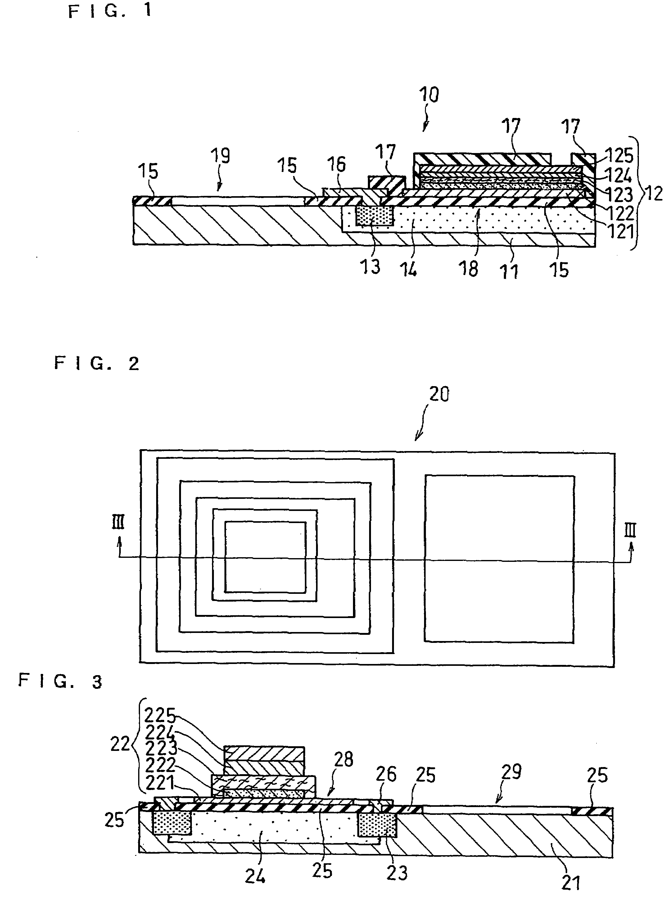
[0021]FIG. 1 shows a battery mounted integrated circuit device in accordance with one embodiment of the present invention.

[0022]The battery mounted integrated circuit device 10 in FIG. 1 comprises a semiconductor substrate 11, and a solid state battery 12 and an integrated circuit (not shown) which are mounted on the semiconductor substrate 11. The battery mounted integrated circuit device 10 further comprises a first diffusion layer 13 containing an N-type impurity, formed between a region 18 of the semiconductor substrate 11 where the solid state battery 12 is mounted and a region 19 of the semiconductor substrate 11 where the integrated circuit is mounted, and a second diffusion layer 14 containing an N-type impurity formed below the region 18 of the semiconductor substrate 11 where the solid state battery 12 is mounted. Herein, an insulating layer 15 is formed on the surface of the semiconductor substrate 11. Further, a wiring layer 16 formed on the semiconductor substrate 11 is...

embodiment 2

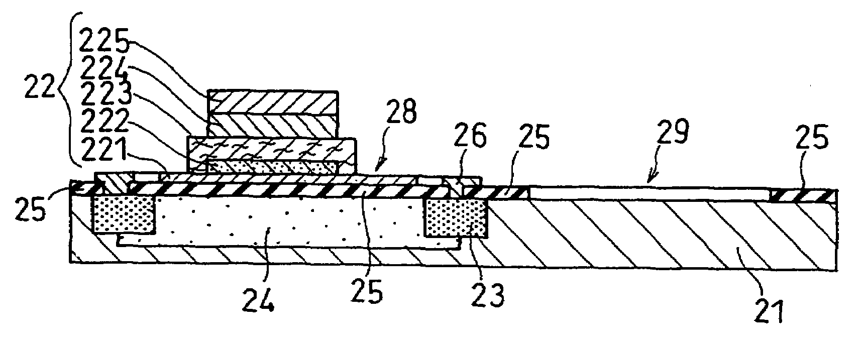
[0065]A description is given to a battery mounted integrated circuit device, where the first diffusion layer is formed so as to surround the region where the solid state battery is mounted, with reference to FIGS. 2 and 3.

[0066]In the battery mounted integrated circuit device 20 in FIG. 2, a solid state battery 22 and an integrated circuit (not shown) are mounted on a semiconductor substrate 21. As shown in FIG. 3, a first diffusion layer 23 containing an N-type impurity is formed between a region 28 of the semiconductor substrate 21 where the solid state battery 22 is mounted and a region 29 of the semiconductor substrate 21 where the integrated circuit is mounted. Further, a second diffusion layer 24 containing the N-type impurity is formed below the region 28 of the semiconductor substrate 21 where the solid state battery 22 is mentioned. Herein, as in the case of Embodiment 1 above, the insulating layer 25 is formed on the surface of the semiconductor substrate 21. Further, the ...

example 1

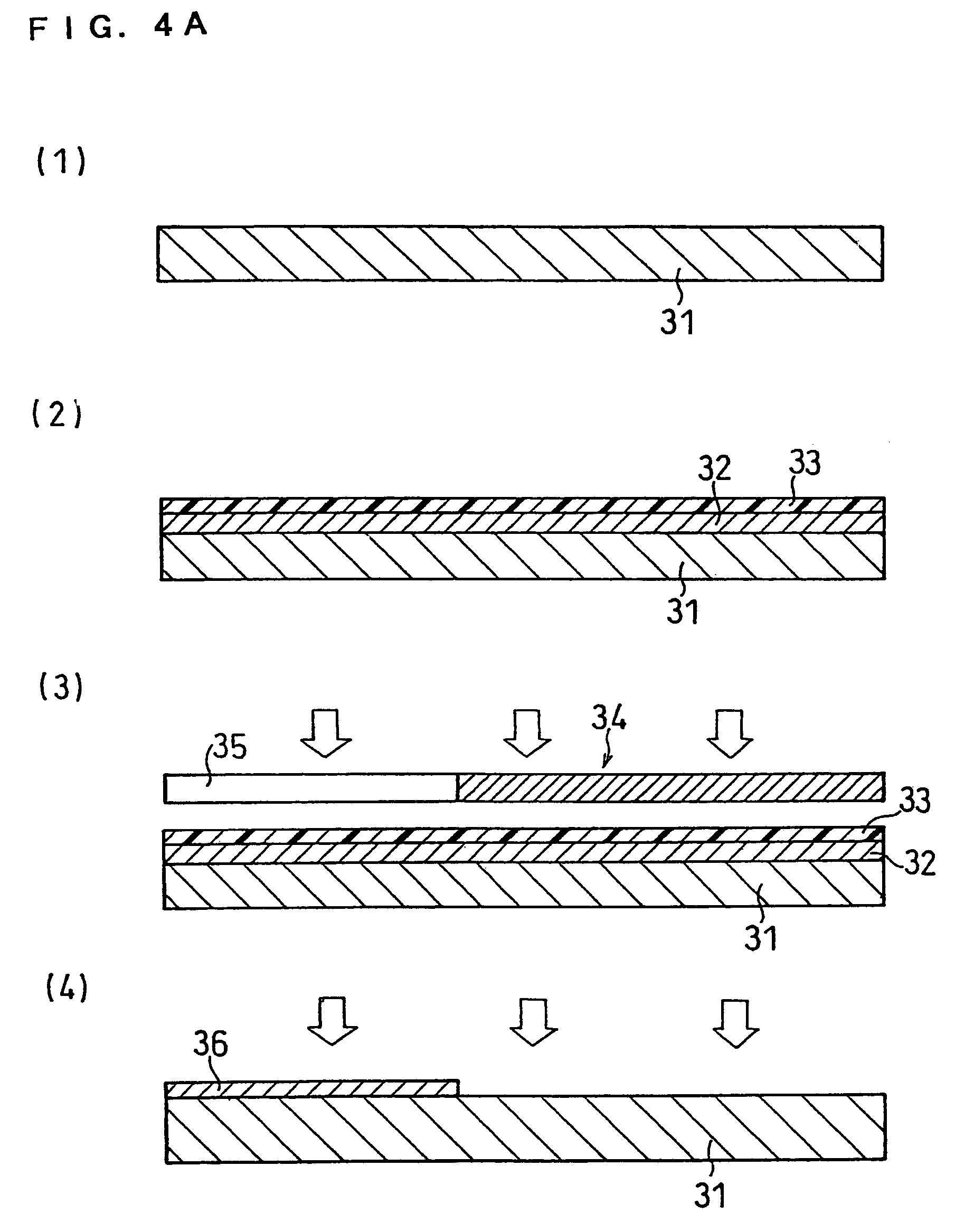
[0074]The battery mounted integrated circuit device as shown in FIG. 1 was produced by the processes shown in FIGS. 4A to 4D. FIGS. 4A to 4D mainly show production methods of the first diffusion layer, the second diffusion layer and the solid state battery.

[0075]On a silicon substrate 31 shown in FIG. 4A (1), a silicon oxide film 32 having a thickness of 1500 Å was formed by the plasma CVD method. Herein, the silicon substrate 31 was P-type and had a diameter of 4 inches, a thickness of 525 μm, and a specific resistance of 10 to 15 Ω·cm. In the plasma CVD method, SiH4 and N2O were used as reactive gases, and these reactive gases were irradiated with a low frequency of 50 kHz frequency at an output of 4 kW to generate plasma. Further, the growth temperature of the silicon oxide film 32 was 380° C.

[0076]A photosensitive resist was applied on the silicon oxide film 32. In this application, a spin coater at a rotation speed of 2000 rpm was used and the applied photosensitive resist had ...


PUM

PropertyMeasurementUnit
thicknessaaaaaaaaaa
thicknessaaaaaaaaaa
thicknessaaaaaaaaaa

Abstract

The present invention relates to a battery mounted integrated circuit device where an integrated circuit and a solid state battery are formed on the same substrate. In this battery mounted integrated circuit device, a first diffusion layer containing an N-type impurity is formed between a region of a semiconductor substrate where the solid state battery is mounted and a region of the semiconductor substrate where the integrated circuit is mounted, and a second diffusion layer containing an N-type impurity is formed below the region of the semiconductor substrate where the solid state battery is mounted, and overlaps with the first diffusion layer.

Description

TECHNICAL FIELD[0001]The present invention relates to a battery mounted integrated circuit device constituted by the coexistence of an integrated circuit and a solid state battery.BACKGROUND ART[0002]In recent years, with size reduction in electronic devices, an all-solid state battery has been formed together with semiconductor devices on a semiconductor substrate. In such a semiconductor substrate, in some cases, ions which serve to charge / discharge a solid state battery, e.g. lithium ions, diffuse to the semiconductor substrate. When those ions having diffused in the semiconductor substrate reach semiconductor devices, there are possibilities that the characteristics of the semiconductor devices deteriorate or the semiconductor devices improperly operate.[0003]Regarding such a battery mounted integrated circuit device as described above where semiconductor devices and a solid state battery are formed on the same semiconductor substrate, as a method for reducing an influence on th...

Claims


Application Information

Patent Timeline
Patent Type & Authority Patents(United States)
IPC IPC(8): H01L29/00H01L23/58H01M10/05H01M10/052H01M10/0561H01M10/0565H01M10/36H01M10/42H01M50/117H01M50/121H01M50/124
CPCH01L23/58H01M2/0275H01M6/40H01M10/05H01M10/052H01M10/4257H01M10/0561H01L2924/0002H01M10/0565Y02E60/122H01L2924/00Y02E60/10H01M50/117H01M50/121H01M50/124
Inventor MINO, SHINJIISHII, HIRONORIUGAJI, MASAYASHIBANO, YASUYUKI
Owner PANASONIC CORP
Why Eureka
Try Eureka