Semiconductor device and driving method of semiconductor device

a semiconductor and driving method technology, applied in the direction of dc-dc conversion, power conversion systems, digital storage, etc., can solve the problems of large size of semiconductor memory devices, large overshoot and ripple, and change of clock signals supplied to the plurality of booster circuits

Inactive Publication Date: 2007-08-07
KK TOSHIBA
View PDF22 Cites 102 Cited by
  • Summary
  • Abstract
  • Description
  • Claims
  • Application Information

AI Technical Summary

Problems solved by technology

When the boosting ability of the booster circuit 12 is elevated, as shown in FIG. 19, there occurs such a problem that overshoot and ripple become large.
Thereby, there arises a problem that, when the frequency of the clock generating circuit itself is changed, the frequencies of all the clock signals supplied to the plurality of booster circuits change.
On the other hand, when clock generating circuits are provided so as to correspond to each of the plurality of booster circuits, there occur such a problem that the size of the semiconductor memory device is made large and such a problem that the amplitude or the frequency of the clock signal is fluctuated.

Method used


Image

  • Semiconductor device and driving method of semiconductor device
  • Semiconductor device and driving method of semiconductor device
  • Semiconductor device and driving method of semiconductor device

Examples


first embodiment

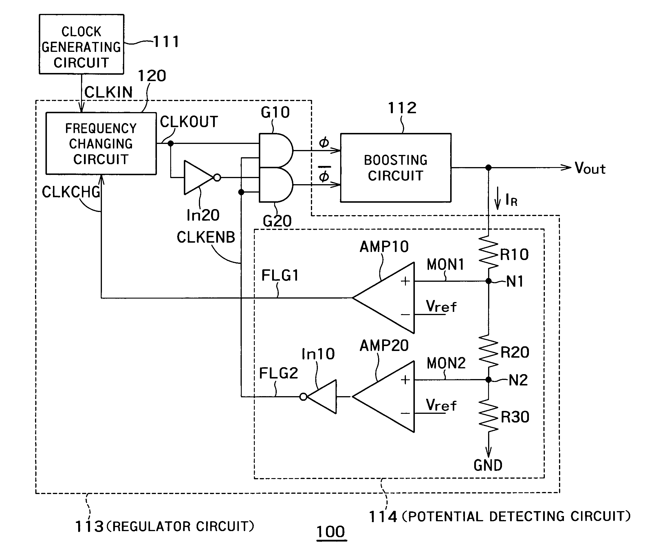
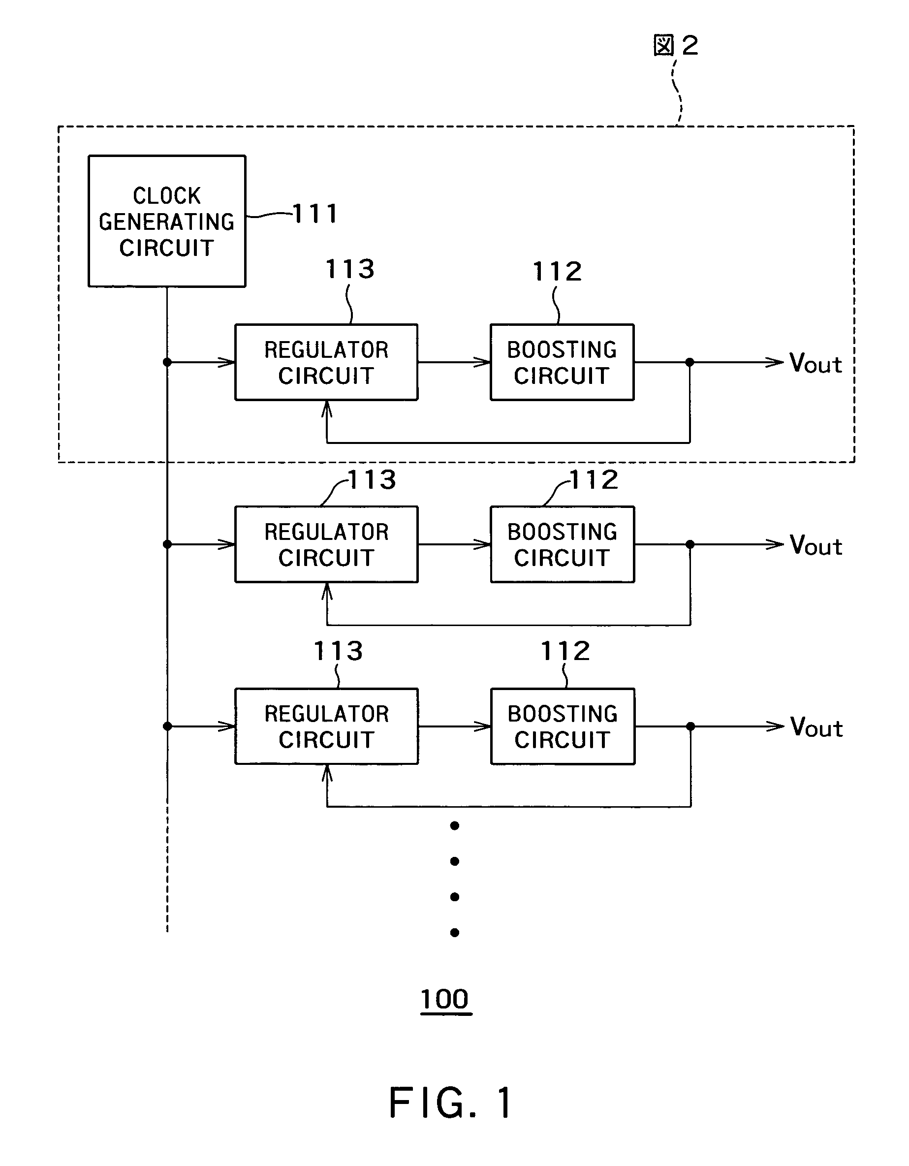
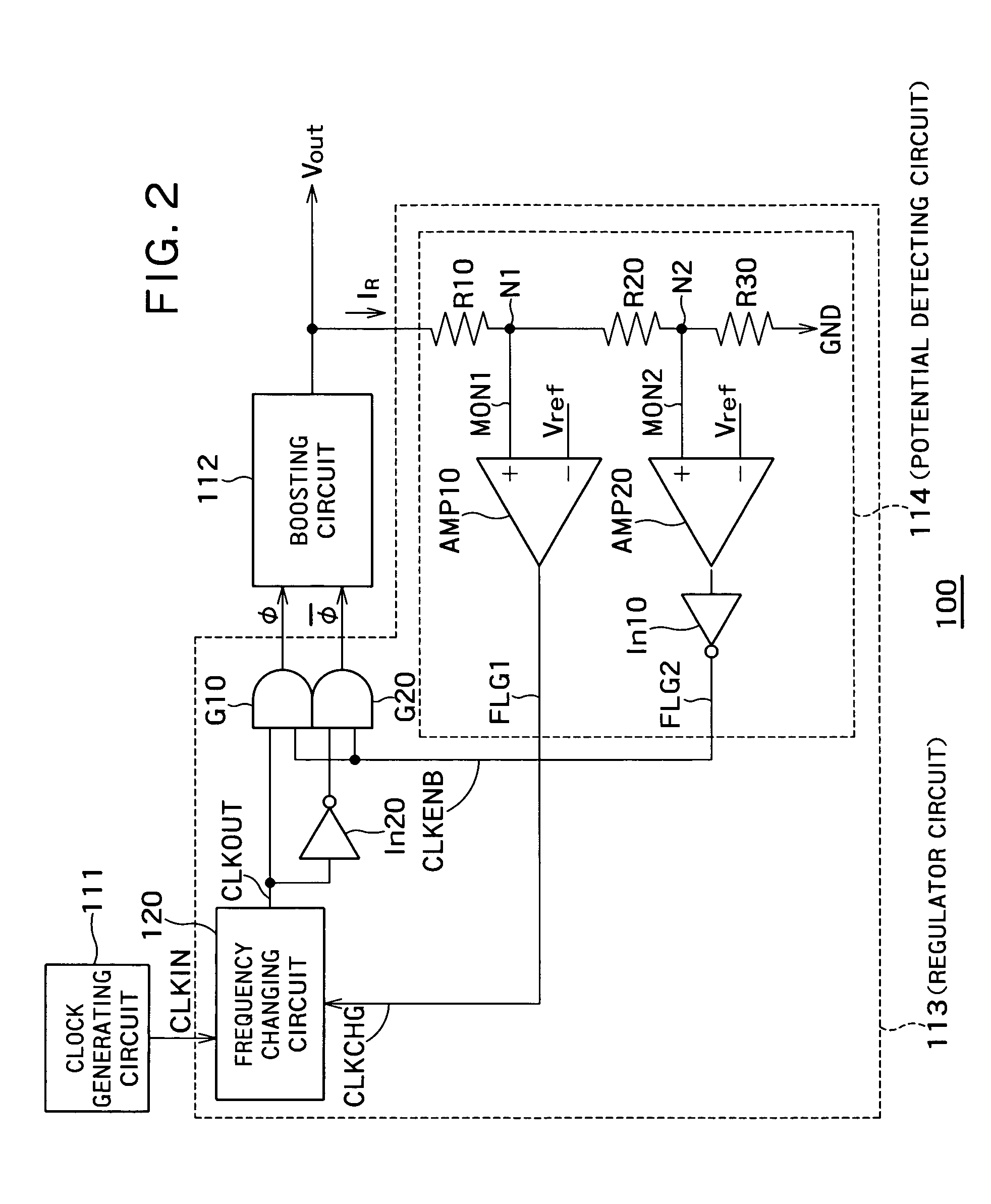
[0037]FIG. 1 is a block diagram of a boosted potential generating section of a semiconductor device 100 according to a first embodiment of the present invention. The semiconductor device 100 is provided with a clock generating circuit 111, booster circuits 112 and regulator circuits 113. Thus, a plurality of the booster circuits 112 are provided to correspond to one clock generating circuit 111. The regulator circuit 113 is provided between each booster circuit 112 and the clock generating circuit 111 so as to correspond to each booster circuit 112. The clock generating circuit 111 may be constituted of an oscillator such as, for example, a ring oscillator. The booster circuit 112 may be a charge pump of Dickson type such as, for example, shown in FIG. 5.

[0038]The clock generating circuit 111 generates a clock signal. The booster circuit 112 boosts a supply voltage using the clock signal and further outputs the boosted supply voltage. The regulator circuit 113 detects an output pote...

second embodiment

[0073]A block diagram of a boosting section of a semiconductor device 200 according to a second embodiment is similar to that in FIG. 1. In this embodiment, a regulator circuit 213 is provided in place of the regulator circuit 113.

[0074]FIG. 9 is a circuit diagram showing a clock generating circuit 111, one of booster circuits 112 and one of regulator circuit 213.

[0075]The regulator circuit 213 includes resistor s R10, R20, R30 and R40, differential amplifiers AMP10, AMP20 and AMP30, a frequency changing circuit 220, a latch circuit 215, and inverters In10, In20, In30 and In40.

[0076]The resistors R10, R20, R30 and R40 are connected in series between an output of the booster circuit 112 and the ground GND. The resistors R10, R20, R30 and R40 may be either fixed resistors or variable resistors. The resistors R10, R20, R30 and R40 potential-divides the output potential Vout to produce a monitor potential MON1 from a node N1 between the resistor R10 and the resistor R20, a monitor poten...

third embodiment

[0106]A block diagram of a boosting section of a semiconductor device 300 according to a third embodiment is similar to that in FIG. 1. Incidentally, in this embodiment, a regulator circuit 313 is provided in place of the regulator circuit 313.

[0107]FIG. 14 is a circuit diagram of a clock generating circuit 111, one of booster circuits 112 and one of regulator circuits 313. The regulator circuit 313 is different from the regulator circuit 113 in that the former is provided with one differential amplifier and it includes a latch circuit 315.

[0108]Resistors R10 and R20 is connected in series between an output of the booting circuit 112 and the ground GND. The resistors R10 and R20 potential-divide an output potential Vout to produce a monitor potential MON1 from a node N1 between the resistor R10 and the resistor R20. Since the monitor potential MON1 changes in proportion to the output potential Vout, the output potential Vout can be monitored.

[0109]One input of a differential amplifi...


PUM


Abstract

A semiconductor device that includes a clock generator which generates a clock signal; a booster which boosts a supply voltage by using the clock signal to output the boosted voltage; a potential detector which detects an output potential of the booster to output a frequency changing signal depending on the output potential; and a frequency changer which is interposed between the clock generator and the booster to change the frequency of the clock signal from the clock generator to the booster on the basis of the frequency changing signal.

Description

CROSS-REFERENCE TO RELATED APPLICATION[0001]This application is based upon and claims the benefit of priority from the prior Japanese Patent Applications No. 2003-429147, filed on Dec. 25, 2003, the entire contents of which are incorporated herein by reference.BACKGROUND OF THE INVENTION[0002]1. Field of the Invention[0003]The present invention relates to a semiconductor device and a driving method of a semiconductor device.[0004]2. Background Art[0005]Such a semiconductor memory device as a NAND type flash memory or the like requires a voltage which is higher than a power source voltage and is constant in order to write, erase or read data. For this reason, a semiconductor device is provided with a booster circuit which boosts a power source and a regulator circuit which holds an output voltage of the booster circuit in a constant voltage.[0006]FIG. 18 shows one example of a boosted potential generating portion in a conventional semiconductor memory device 10. A clock generating ci...

Claims


Application Information

Patent Timeline
Patent Type & Authority Patents(United States)
IPC IPC(8): G05F1/10G11C16/06G11C7/00G11C11/40H02M3/07
CPCH02M3/073G11C5/143G11C5/147G11C7/222G11C16/0483G11C16/30
Inventor FUKUDA, KOICHIIMAMIYA, KENICHI
Owner KK TOSHIBA
Why Eureka
Try Eureka