Programmable memory device, integrated circuit including the programmable memory device, and method of fabricating same

a programmable memory and integrated circuit technology, applied in the direction of semiconductor devices, electrical devices, transistors, etc., can solve the problems of increasing the number of processes for completing the ic, the process required to embed the cell of the otp memory device within the stack structure shown in fig. 1 through 3 in the existing integrated circuit (ic) is complicated, and the cost of fabricating the ic increases

Inactive Publication Date: 2007-08-21
SAMSUNG ELECTRONICS CO LTD
View PDF22 Cites 18 Cited by
  • Summary
  • Abstract
  • Description
  • Claims
  • Application Information

AI Technical Summary

Benefits of technology

[0011]A one-time programmable memory device, according to an embodiment of the present invention, includes an isolation layer for defining an active area of a substrate, an oxide layer formed on the active area, a floating gate formed over the active area and the isolation layer, an inter-gate dielectric layer formed on the floating gate, and a control gate formed on the inter-gate dielectric layer.

Problems solved by technology

The process required to embed a cell of an OTP memory device within the stack structure shown in FIGS. 1 through 3 in an existing integrated circuit (IC) is complicated.
When using an OTP memory device having the stacked structure, the number of processes for completing the IC increases and the cost of fabricating the IC increases.
Thus, the reliability of the MOS transistor may deteriorate.

Method used


Image

  • Programmable memory device, integrated circuit including the programmable memory device, and method of fabricating same
  • Programmable memory device, integrated circuit including the programmable memory device, and method of fabricating same
  • Programmable memory device, integrated circuit including the programmable memory device, and method of fabricating same

Examples


Embodiment Construction

[0032]Preferred embodiments of the present invention will be described below in more detail with reference to the accompanying drawings. This invention may, however, be embodied in different forms and should not be construed as being limited to the embodiments set forth herein. Rather, these embodiments are provided so that this disclosure will be thorough and complete, and will fully convey the scope of the invention to those skilled in the art. In the drawings, the forms of elements may be exaggerated for clarity. To facilitate understanding, identical reference numerals have been used, where possible, to designate identical elements that are common to the figures.

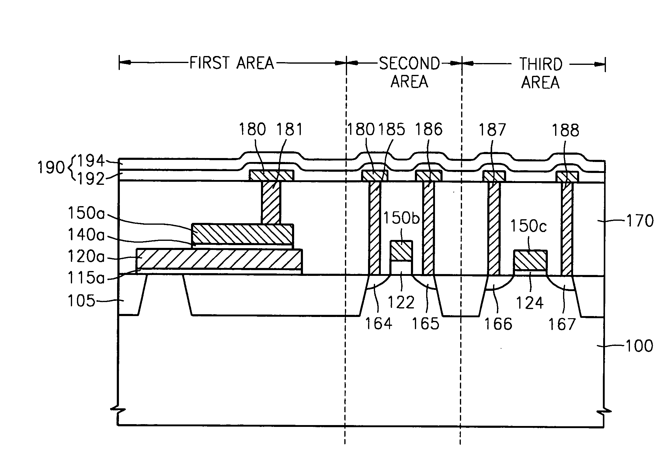
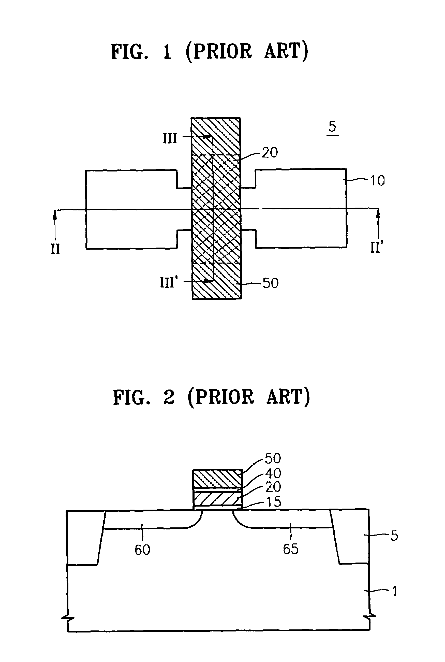
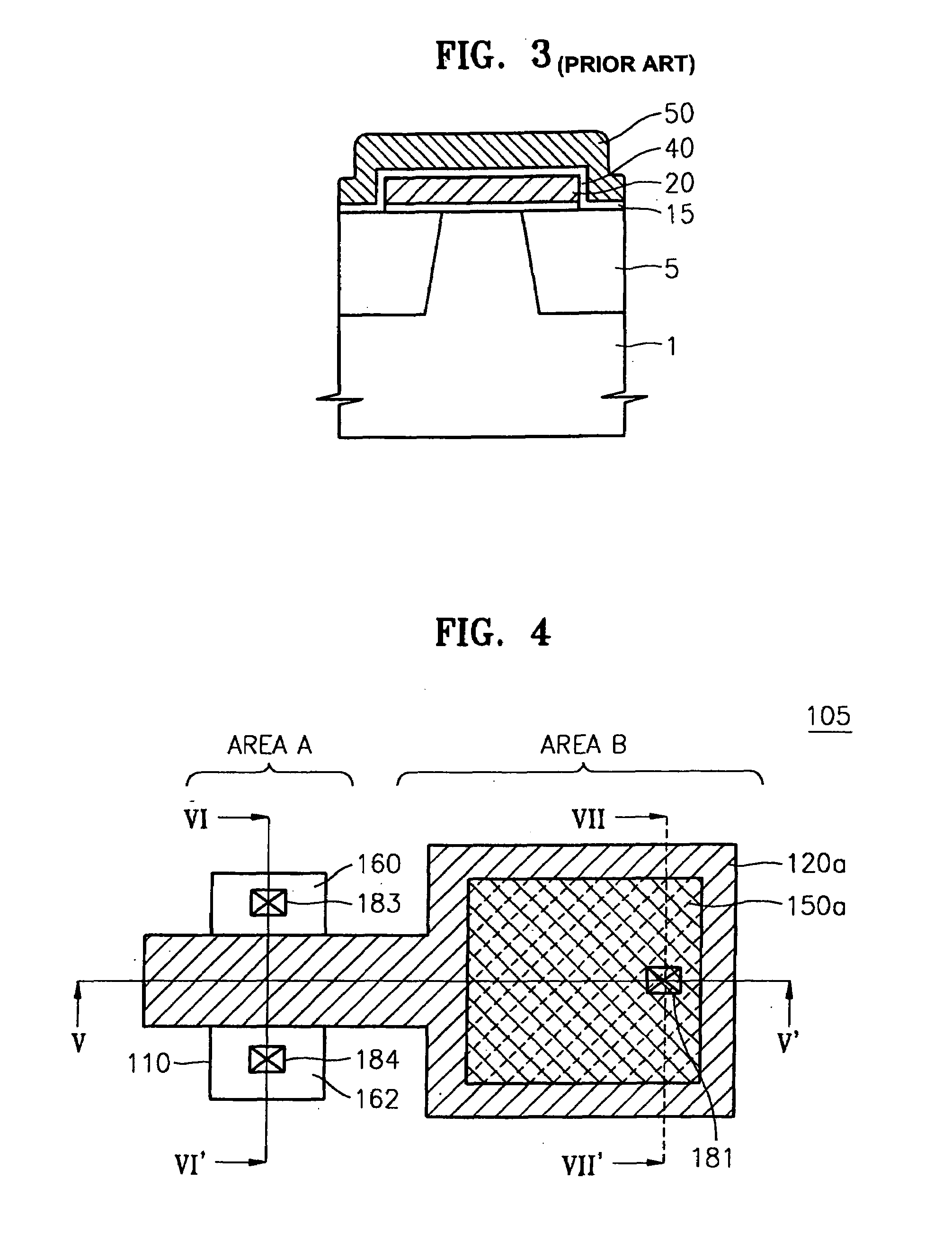
[0033]FIG. 4 is a layout view of a one-time programmable memory device according to an embodiment of the present invention. FIG. 5 is a cross-sectional view taken along line V-V′ of FIG. 4. FIG. 6 is a cross-sectional view taken along line VI-VI′ of FIG. 4. FIG. 7 is a cross-sectional view taken along line VII-VII′ of FI...


PUM


Abstract

An integrated circuit comprises a memory device including an isolation layer for defining an active area of a substrate, a tunnel oxide layer formed on the active area, a floating gate formed over the active area and the isolation layer, an inter-gate dielectric layer formed on the floating gate, and a control gate formed on the inter-gate dielectric layer. The integrated circuit also includes a high and low voltage transistors.

Description

BACKGROUND OF THE INVENTION[0001]This application claims the priority of Korean Patent Application No. 2003-33346, filed on May 26, 2003, in the Korean Intellectual Property Office, the disclosure of which is incorporated herein in its entirety by reference.[0002]1. Technical Field[0003]The present disclosure relates to a nonvolatile memory device and a method of fabricating same. More particularly, the present invention relates to a one-time programmable (OTP) memory device and a method of fabricating the OTP memory device.[0004]2. Discussion of the Related Art[0005]Nonvolatile memory devices are devices from which data is not erased even with discontinued power and which are used to selectively program data according to the needs of a user. OTP memory devices are used for programming data only one time without erasing or adding data. Demand for OTP memory devices has been increasing.[0006]A cell area of an OTP memory device may have a layout as shown in FIG. 1. FIG. 2 is a cross-s...

Claims


Application Information

Patent Timeline
Patent Type & Authority Patents(United States)
IPC IPC(8): H01L29/76H01L27/10H01L21/336H01L21/82H01L21/8247H01L27/02H01L27/105H01L27/115H01L29/423H01L29/788H01L29/792
CPCH01L27/105H01L27/11526H01L27/11546H01L29/42324H01L29/66825H10B41/40H10B41/49H10B99/00
Inventor KOO, JEOUNG-MOOH, HEE-SEON
Owner SAMSUNG ELECTRONICS CO LTD
Why Eureka
Try Eureka