Method of manufacturing semiconductor devices

a manufacturing method and technology of semiconductor devices, applied in semiconductor/solid-state device manufacturing, basic electric elements, electric devices, etc., can solve the problems of degrading affecting and not completely removing the photoresist film, etc., to achieve the effect of improving the reliability of the gate oxide film

Inactive Publication Date: 2004-12-07
KEY FOUNDRY CO LTD
View PDF16 Cites 4 Cited by
  • Summary
  • Abstract
  • Description
  • Claims
  • Application Information

AI Technical Summary

Benefits of technology

Accordingly, to substantially obviate one or more problems described above, a method of manufacturing semiconductor devices is disclosed by which a photoresist film remnant does not remain after the removal process of the photoresist film, thereby improving reliability of a gate oxide film.
The disclosed method can also prevent a reduction in the breakdown voltage characteristic due to grain protrusion of polysilicon.

Problems solved by technology

However, in the process of removing the photoresist film using ozone plasma, the photoresist film is not completely removed and remnants remain.
This degrades reliability of the gate oxide film and the plasma also damages the gate oxide film.
Further, while the method of forming the polysilicon film by applying vacuum four times is good for dopant channeling prevention, as the grain protrusion of the polysilicon film penetrates into the gate oxide film, however, an interfacial roughness between the gate oxide film and polysilicon increases, thereby increasing the leakage current at a pre-tunneling region.
Further, if the polysilicon film is formed by the above method, the process time is increased because of the multiple vacuum treatments required.

Method used


Image

  • Method of manufacturing semiconductor devices
  • Method of manufacturing semiconductor devices
  • Method of manufacturing semiconductor devices

Examples


Embodiment Construction

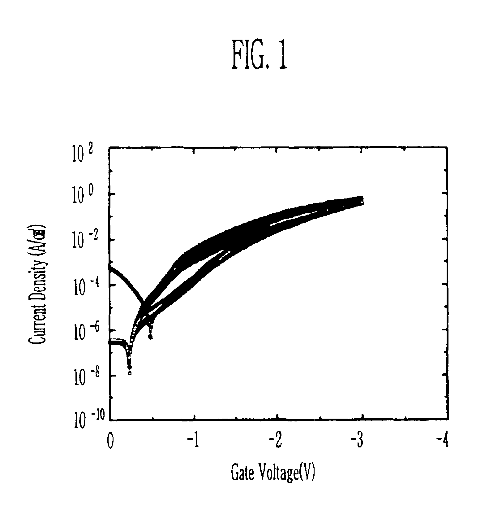
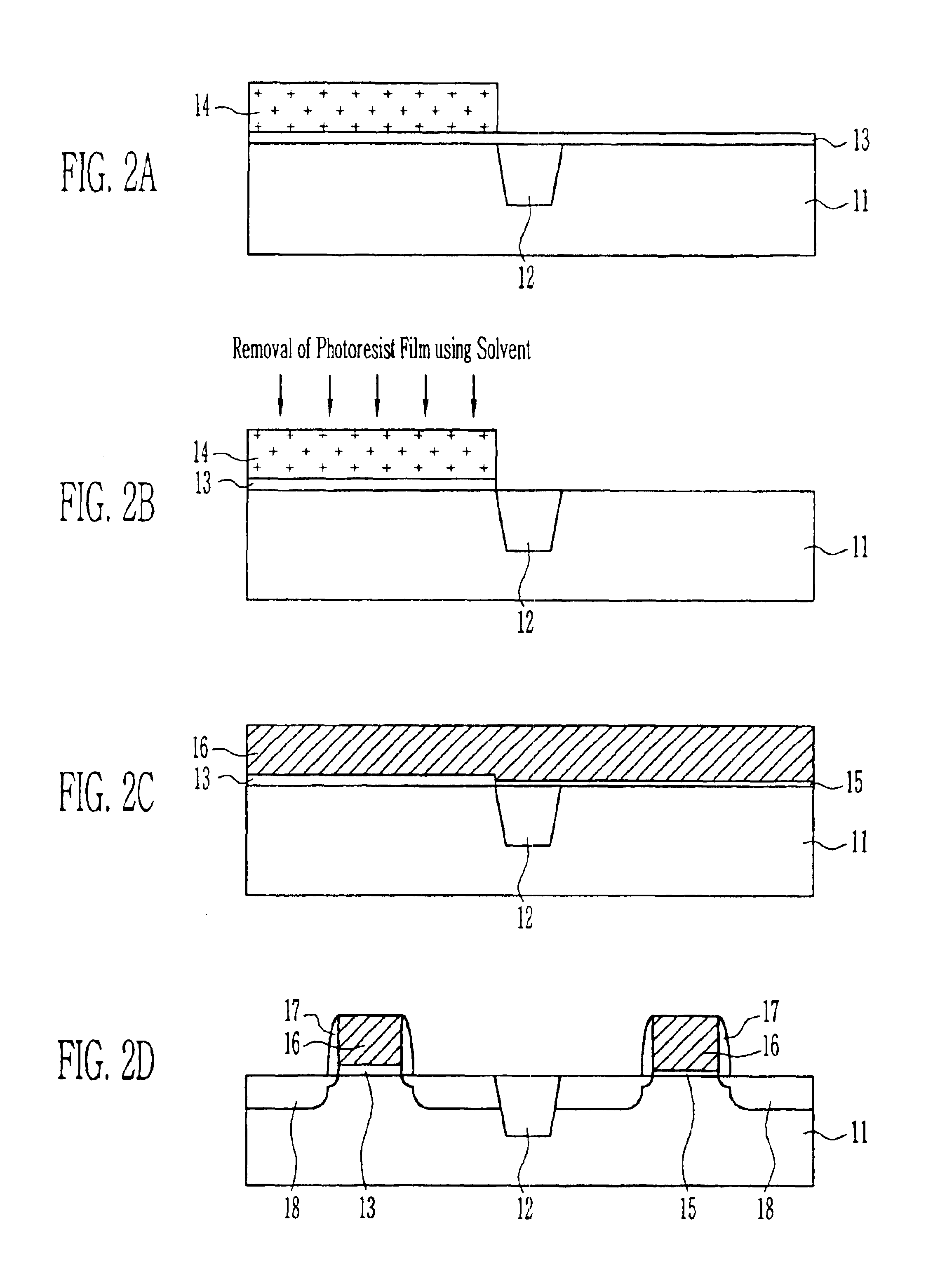
Reference will now be made in detail to the preferred embodiments of the present invention, examples of which are illustrated in the accompanying drawings, in which like reference numerals are used to identify the same or similar parts. FIG. 2A-FIG. 2D are cross-sectional views of semiconductor devices for explaining a method of manufacturing the device according to a preferred embodiment.

Referring to FIG. 2A, an isolation film 12 is formed at a given region of a semiconductor substrate 11 to define a high voltage device region and a low voltage device region. An ion implantation process is then performed to form a well region. Next, the semiconductor substrate 11 is precleaned using a HF solution diluted with a mixture solution of NH.sub.4 OH / H.sub.2 O.sub.2 / H.sub.2 O. Thereafter, a first oxide film 13 is thickly formed on the entire structure. At this time, the first oxide film 13 is formed by oxidizing the semiconductor substrate 11 using vaporized H.sub.2 O generated by pyrolys...


PUM


Abstract

Disclosed is a method of manufacturing semiconductor devices. In the process of simultaneously forming a high voltage device and a low voltage device, a photoresist film for patterning a gate oxide film in a high voltage device is removed in a wet mode using a solvent. The polysilicon film used as the gate electrode is then formed without applying a vacuum. It is thus possible to increase reliability of the gate oxide film, and prevent damage of the gate oxide film due to ozone plasma and penetration of a grain protrusion of the polysilicon film into the gate oxide film. Accordingly, the breakdown voltage characteristic of the gate oxide film is improved.

Description

1. Technical FieldA method of manufacturing semiconductor devices is disclosed, wherein a process of simultaneously forming a high voltage device and a low voltage device is carried out. More specifically, a photoresist film for patterning a gate oxide film in a high voltage device is removed in a wet mode using a solvent and the polysilicon film used as the gate electrode is formed without applying vacuum, whereby reliability of the gate oxide film is increased, damage of the gate oxide film due to ozone plasma is prevented and penetration of a grain protrusion of the polysilicon film into the gate oxide film is prevented, thus improving the breakdown voltage characteristic of the gate oxide film.2. Background of the Related ArtIn semiconductor devices in which a high voltage device operating at a high voltage and a low voltage device operating at a low voltage are simultaneously fabricated, the gate oxide film in the high voltage device is made thicker than the gate oxide film in ...

Claims


Application Information

Patent Timeline
Patent Type & Authority Patents(United States)
IPC IPC(8): H01L21/70H01L21/8234H01L21/336H01L21/306H01L21/311
CPCH01L21/823462H01L21/31133H01L21/02052H01L21/18
Inventor CHO, IHL HYUN
Owner KEY FOUNDRY CO LTD
Why Eureka
Try Eureka