Silicon carbide mosfet device and method for manufacturing the same

a silicon carbide mosfet and mosfet technology, applied in the field of silicon carbide mosfet devices, can solve the problems of serious affecting the reliability of the gate oxide layer, significant electric field curvature, and the device can reach 2 mv/cm to 3 mv, so as to improve voltage resistance ability, gate oxide layer reliability, and effective reduction of electric field strength.

Active Publication Date: 2019-01-24
ZHUZHOU CSR TIMES ELECTRIC CO LTD
View PDF0 Cites 4 Cited by
  • Summary
  • Abstract
  • Description
  • Claims
  • Application Information

AI Technical Summary

Benefits of technology

[0009]According to one preferred embodiment of the present disclosure, the silicon carbide MOSFET device is a Vertical Double-diffused MOSFET. That is, according to this embodiment, the silicon carbide MOSFET device has a basic structure and a basic operating principle of the Vertical Double-diffused MOSFET well known to those skilled in the art. On this basis, the silicon carbide MOSFET device provided herein has improved structure and performance.
[0014]According to one preferred embodiment of the present disclosure, the gate oxide layer above the channel is arranged to have a small thickness, and thus it can be ensured that the device has a suitable threshold voltage and a good gate control property; while the gate oxide layer above the JFET region is arranged to have a large thickness, so that an electric field strength of the gate oxide layer may be effectively reduced when the device works at a high voltage, and reliability of the gate oxide layer may be improved. According to this technical solution, the JFET region can be arranged to have a relatively large width so as to ensure a low on-resistance of the device.
[0017]The JFET region of the MOSFET device is a region which is arranged adjacent to and side by side with the P well on the N-type epitaxial layer (also called as “N− drift layer”). Specifically, the JFET region is a region between two adjacent P well regions after P wells are formed on an N drift region. According to one preferred embodiment of the present disclosure, the width of the JFET region of the device is in a range from 2 μm to 6 μm, preferably in a range from 3 μm to 5.5 μm, more preferably in a range from 3.2 μm to 5 μm, such as 3.5 μm, 3.8 μm, 4.0 μm, 4.5 μm, 5.0 μm, or 5.5 μm. In order to inhibit electric field concentration in the gate oxide layer of the device, in a traditional silicon carbide MOSFET device, the JFET region is arranged to have a small width, which is usually in a range from 2 μm to 3.5 μm. However, with respect to the silicon carbide MOSFET device provided herein, since the thickness of the gate oxide layer above the channel and the thickness of the gate oxide layer above the JFET region are arranged to be different, the width of the JFET region can be increased (such as 4.0 μm or above) so as to reduce the on-resistance of the device and avoid early breakdown of the device.
[0067]According to one preferred embodiment of the present disclosure, the gate oxide layer medium formed for the second time is formed through the dry thermal oxidation technology, while the gate oxide layer medium formed for the first time is formed through the low pressure chemical vapor deposition technology, or the wet thermal oxidation technology. In this manner, the first gate oxide layer can have a higher compactness compared with the second gate oxide layer, which is conducive to stability of the threshold voltage and the gate oxide layer, and operating reliability of the device. As to the gate oxide layer medium (for forming the second gate oxide layer) formed for the first time, it is unnecessary to use the dry thermal oxidation technology, so that not only a manufacturing difficulty may be reduced, but also a technological cost and a time cost thereof may be saved.
[0068]According to the method for manufacturing the silicon carbide MOSFET device provided herein, selective etching and second-time thermal oxidation growth of the gate oxide layer are adopted to form the gate oxide layer with a staircase shape, whereby a voltage-resistance of the silicon carbide MOSFET device may be improved, an on-resistance thereof may be reduced, and other performances thereof may be improved.
[0088]The silicon carbide MOSFET device provided herein has an improved gate oxide layer with a specific structure, i.e., a staircase-shaped gate oxide layer. Specifically, the gate oxide layer above the JFET region is arranged to have a large thickness, while the gate oxide layer above the channel is arranged to have a small thickness. In this manner, the electric field strength of the gate oxide layer can be effectively reduced, and the threshold voltage and the gate control property of the device would not be affected. That is, under a condition that the threshold voltage and the on-resistance of the device are not increased, a voltage-resistance ability and reliability of the gate oxide layer can be improved. Therefore, other parameters of the device can be arranged in a larger scope. For example, the JFET region can be arranged to have a larger width to further reduce the on-resistance of the device to 8 mΩ·cm2 or below, or even 6 mΩ·cm2 or below.

Problems solved by technology

However, it should be noted that, a critical breakdown electric field strength of the silicon carbide MOSFET device can reach 2 MV / cm to 3 MV / cm, which is different from the silicon-based MOSFET device.
According to the principle of continuity of electric flux at oxide interface, when the device works at a high voltage, an electric field strength of a gate oxide layer above a JFET (Junction Field Effect Transistor) region may easily exceed 4 MV / cm, which seriously affects reliability of the gate oxide layer.
With respect to a silicon carbide MOSFET power device, if a width of the JFET region is too small, an on-resistance thereof will become over large; while if the width thereof is too large, a concentrated effect of an electric field curvature will become significant, and a breakdown voltage of the device will drop.
However, according to the improvement methods in the prior art, on the one hand, the on-resistance of the device would be increased; and on the other hand, high-dose of Al ions need to be injected therein using high energy, which increase manufacturing difficulty thereof, and is not conducive to reduction of the working loss.

Method used


Image

  • Silicon carbide mosfet device and method for manufacturing the same
  • Silicon carbide mosfet device and method for manufacturing the same
  • Silicon carbide mosfet device and method for manufacturing the same

Examples


embodiment 1

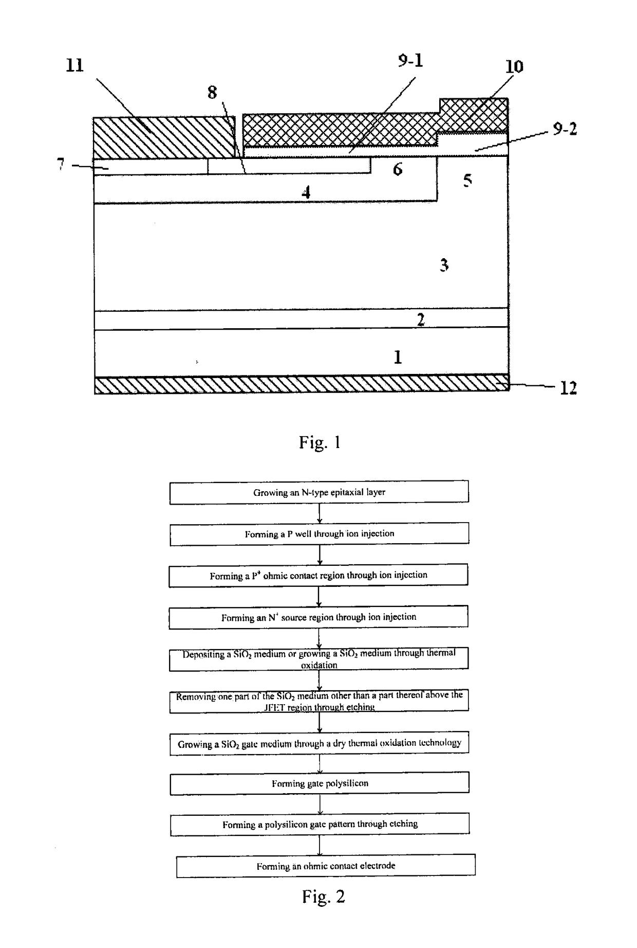
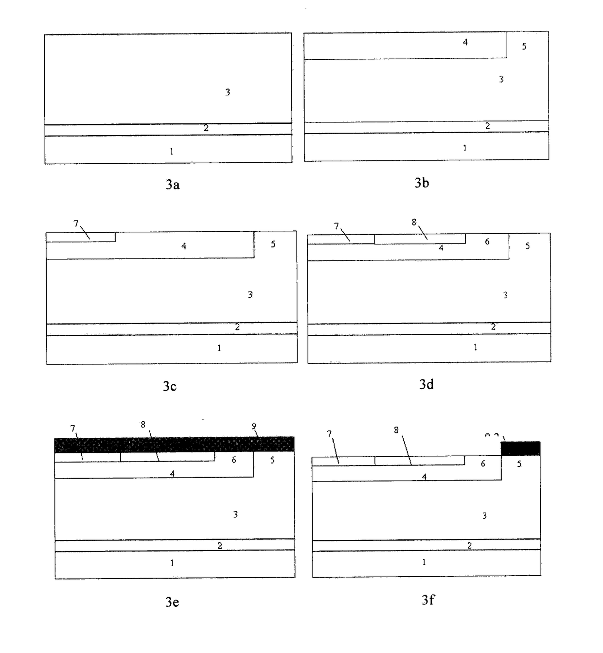
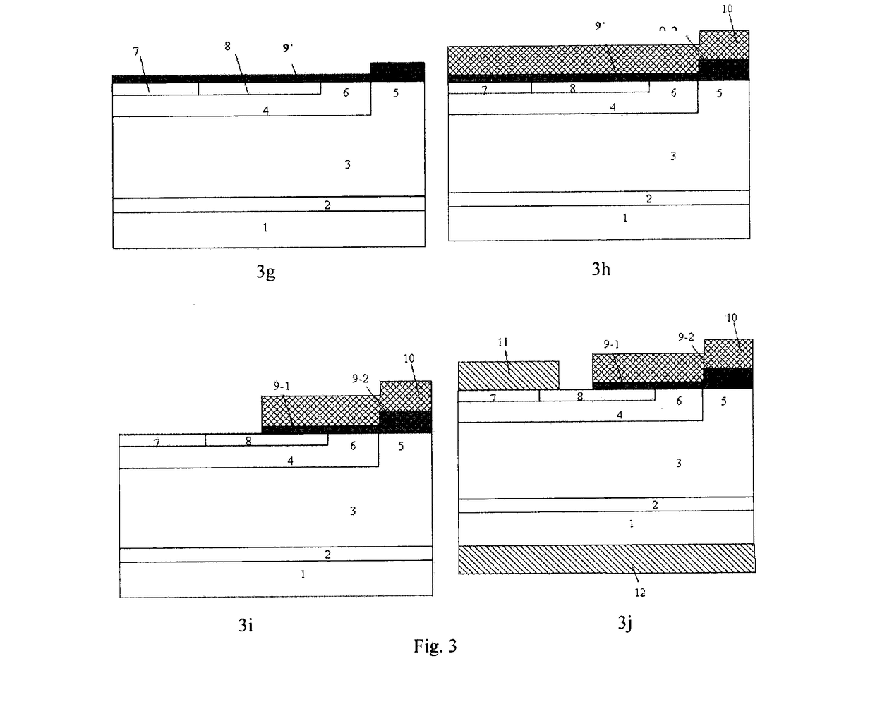
[0129]A silicon carbide MOSFET device a is manufactured through the aforesaid method, and a voltage-resistance level of the device is 1200 V. The parameters of each of the parts of the device are as follows: the thickness of the N-type buffer layer that is formed on the silicon carbide substrate is 1 μm; the thickness of the N-type epitaxial layer is 12 μm, and the N ion doping concentration thereof is 8.5×105 cm−3; the junction depth of the P well is 0.9 μm, and the Al ion doping concentration thereof is 1×1018 cm−3; the junction depth of the P+ doped region is 0.3 μm, and the Al ion doping concentration thereof is 1×1019 cm−3; the junction depth of the N+ source region is 0.3 μm, and the N ion doping concentration thereof is 1×1019 cm−3; the width of the JFET region is 3 μm; the width of the channel is 1 μm; the width of the second gate oxide layer, and the width of the first gate oxide layer are respectively 3 μm and 10 μm, and the thicknesses thereof are respectively 120 nm and ...

embodiment 2

[0131]A silicon carbide MOSFET device b is manufactured through a similar method, and a voltage-resistance level of the device is 1200 V. Device b differs from device a in that: the width of the JFET region is 5 μm; and the width of the second gate oxide layer, and the width of the first gate oxide layer are respectively 5 μm and 10 μm, and the thicknesses thereof are respectively 120 nm and 60 nm.

[0132]Similar to embodiment 1, an electrical property simulation is performed on device b, and it can be obtained that, when the device b works at a blocking voltage 1200 V, a peak electric field strength of the gate oxide layer above the JFET region is 1.5 MV / cm, and electric field concentration phenomenon can be effectively inhibited. When the device works in an on-state, an on-resistance thereof is 5.3 mΩ·cm2 under a 1.6 V positive voltage drop. The on-resistance of device b is lower than that of device a.

embodiment 3

[0133]A silicon carbide MOSFET device c is manufactured through a similar method, and a voltage-resistance level of the device is 1200 V. The parameters of each of the parts of the device are as follows: the thickness of the N-type buffer layer that is formed on the silicon carbide substrate is 1 μm; the thickness of the N-type epitaxial layer is 10 μm, and the N ion doping concentration thereof is 6×1015 cm−3; the junction depth of the P well is 0.9 μm, and the Al ion doping concentration thereof is 1×1018 cm−3; the junction depth of the P+ doped region is 0.3 μm, and the Al ion doping concentration thereof is 1×1019 cm−3; the junction depth of the N+ source region is 0.3 μm, and the N ion doping concentration thereof is 1×1019 cm−3; the width of the JFET region is 3 μm; the width of the channel is 1 μm; the width of the second gate oxide layer, and the width of the first gate oxide layer are respectively 2 μm and 10 μm, and the thicknesses thereof are respectively 150 nm and 50 nm...


PUM


Abstract

A silicon carbide MOSFET device is disclosed. The silicon carbide MOSFET device includes a gate oxide layer which is constituted by a first gate oxide layer and a second gate oxide layer. A thickness of the second gate oxide layer is larger than a thickness of the first gate oxide layer. Through dividing the gate oxide layer into two parts with different thicknesses, i.e., enabling the gate oxide layer to have a staircase shape, an electric field strength of the gate oxide layer can be effectively reduced, while a threshold voltage and a gate control property of the device are not affected. An on-resistance of the device can be reduced through increasing a width of a JFET region. A method for manufacturing the silicon carbide MOSFET device is further disclosed.

Description

CROSS REFERENCE TO RELATED APPLICATIONS[0001]The present application claims the priority of Chinese patent application CN201510274919.4, entitled “Silicon Carbide MOSFET Device and Method for Manufacturing the Same” and filed on May 26, 2015, the entirety of which is incorporated herein by reference.FIELD OF THE INVENTION[0002]The present disclosure relates to the technical field of semiconductors, specifically to a power device, and particularly to a silicon carbide MOSFET device and a method for manufacturing the same.BACKGROUND OF THE INVENTION[0003]Compared with a first generation of semiconductors with silicon (Si) as a typical example and a second generation of semiconductors with gallium arsenide (GaAs) as a typical example, silicon carbide material, as a typical one of a third generation of semiconductors, has a larger band gap and a higher critical breakdown electric field strength, and is thus suitable to produce high-voltage large-power semiconductor devices. As a researc...

Claims


Application Information

Patent Timeline
Patent Type & Authority Applications(United States)
IPC IPC(8): H01L29/423H01L29/16H01L29/66H01L29/167H01L29/06H01L29/78H01L21/04H01L21/02
CPCH01L29/42368H01L29/1608H01L29/66068H01L29/167H01L21/02255H01L29/7803H01L21/049H01L21/02164H01L21/02236H01L29/0684H01L29/78H01L29/7802
Inventor GAO, YUNBINLI, CHENGZHANLIU, GUOYOUWU, YUDONGSHI, JINGJINGZHAO, YANLI
Owner ZHUZHOU CSR TIMES ELECTRIC CO LTD
Why Eureka
Try Eureka