Mixed-voltage I/O buffer to limit hot-carrier degradation

a buffer and mixed voltage technology, applied in the field of input and output buffers, can solve the problems of unwanted leakage current paths, increased hot-carrier degradation, and lowered gate-oxide reliability, and achieve the effect of increasing the gate-oxide reliability of its internal transistors and high/low voltage tolerance characteristics

Inactive Publication Date: 2009-01-01
AMAZING MICROELECTRONICS
View PDF6 Cites 5 Cited by
  • Summary
  • Abstract
  • Description
  • Claims
  • Application Information

AI Technical Summary

Benefits of technology

[0023]Accordingly, the present invention is directed to an Mixed-voltage input and output (I/O) buffer. The Mixed-voltage I/O buffer has a high/low voltage tolerance characteristic, and regardless of whether the Mixed-voltage I/O buffer is in a...

Problems solved by technology

Because the chip is designed using transistors with a small dimension, a number of problems will arise when the chip is overstressed, for example, gate-oxide reliability may be lowered, hot-carrier degradation may intensify and unwanted leakage current paths may be generated.
Therefore, the transistor N0 and the transistor inside the input buffer 103 may have gate-oxide reliability problem, and the excess voltage between the drain and the source of the transistor N0 may lead to hot-carrier degradation problem.
However, when the I/O buffer 200 makes a transition from receiving a high voltage (for example: 2×VDD) input signal to transmitting a low logic level (for example: 0V) output signal, the stacked transistors MN0 and MN3 used by the I/O ...

Method used


Image

  • Mixed-voltage I/O buffer to limit hot-carrier degradation
  • Mixed-voltage I/O buffer to limit hot-carrier degradation
  • Mixed-voltage I/O buffer to limit hot-carrier degradation

Examples


Embodiment Construction

[0039]Reference will now be made in detail to the present preferred embodiments of the invention, examples of which are illustrated in the accompanying drawings. Wherever possible, the same reference numbers are used in the drawings and the description to refer to the same or like parts.

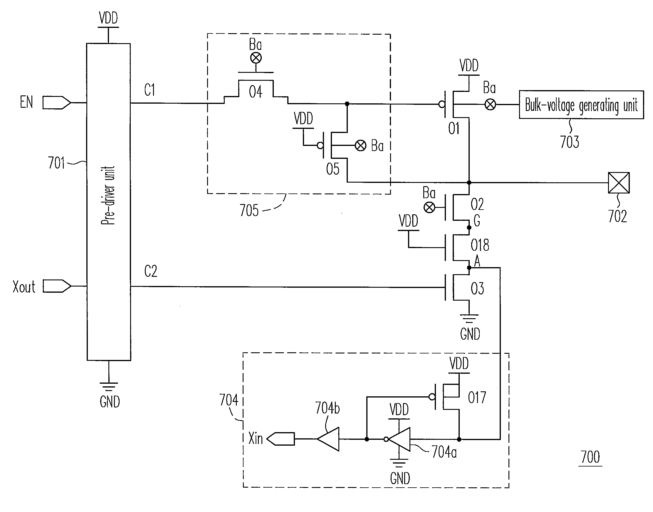
[0040]FIG. 4 is a diagram of an Mixed-voltage input and output buffer according to an embodiment of the present invention. As shown in FIG. 4, the Mixed-voltage input and output (I / O) buffer 400 includes a pre-driver unit 401, a bulk-voltage generating unit 403, an input stage unit 404 and transistors M1˜M3. The transistor M1 is a P-type transistor and the transistors M2˜M3 are N-type transistors. The pre-driver unit 401 outputs a first signal C1 and a second signal C2. The bulk-voltage generating unit 403 determines whether a first voltage (a system voltage VDD) or a pad voltage is connected to the output to be used as a bulk voltage Ba according to the voltage level of the pad 402.

[0041]A gate of t...


PUM


Abstract

A Mixed-voltage input and output (I/O) buffer including a pre-driver unit, a bulk-voltage generating unit, a first to a third transistors and an input stage unit is provided. The pre-driver unit outputs a first source/drain and a second signal. The bulk-voltage generating unit determines whether a first voltage or a pad voltage is used as a bulk voltage according to the pad voltage level. A gate of the first transistor receives the first signal, and a bulk, a first source/drain and a second source/drain of the first transistor are respectively coupled to the bulk voltage, the first voltage and the pad. A gate of the third transistor receives the second signal, and a first source/drain and a second source/drain of the third transistor are respectively coupled to the input stage unit for receiving an input signal from the pad and a second voltage.

Description

BACKGROUND OF THE INVENTION[0001]1. Field of the Invention[0002]The present invention generally relates to an input and output (I / O) buffer, and more particularly, to a mixed-voltage I / O buffer that can limit hot-carrier degradation.[0003]2. Description of Related Art[0004]With the rapid development of complementary metal oxide semiconductor techniques, the dimension of a transistor continues to decrease so as to reduce chip area and fabrication cost and increase operating speed and power performance. However, the source voltage needed to drive the chip also decreases correspondingly. If a voltage higher than the source voltage is used in a signal transmission process, then two different voltage levels coexist when the chip operates so that the higher voltage can overstress the chip.[0005]Because the chip is designed using transistors with a small dimension, a number of problems will arise when the chip is overstressed, for example, gate-oxide reliability may be lowered, hot-carrier...

Claims


Application Information

Patent Timeline
IPC IPC(8): H03K19/0175
CPCH03K19/00315
Inventor KER, MING-DOUTSAI, HUI-WENJIANG, RYAN HSIN-CHIN
Owner AMAZING MICROELECTRONICS
Why Eureka
Try Eureka