Method for producing semiconductor device

a technology of semiconductor devices and gate oxide films, which is applied in the direction of semiconductor devices, basic electric elements, electrical appliances, etc., can solve the problems of adversely affecting the silicon interface, undesirably deteriorating the reliability of the gate oxide films and the performance of the transistor, etc., to achieve stable fixed charge and interface level, high reliability, and high reliability of the semiconductor devi

Inactive Publication Date: 2005-10-13
ELPIDA MEMORY INC
View PDF23 Cites 9 Cited by
  • Summary
  • Abstract
  • Description
  • Claims
  • Application Information

AI Technical Summary

Benefits of technology

[0017] In the method for producing a semiconductor device according to the present invention, the step of annealing at high temperature in a noble gas atmosphere may be added in the process after the growth of a buried oxide film until the growth of a gate polysilicon to round STI corners at the boundary between isolation and active regions. Further, the step of annealing in a noble gas atmo

Problems solved by technology

These corners therefore undesirably deteriorate the reliability of the gate oxide film and the performance of the transistor.
In the above-related art, however, nitrogen contained in the oxynitride film acts as positive charges to adverse

Method used


Image

  • Method for producing semiconductor device
  • Method for producing semiconductor device
  • Method for producing semiconductor device

Examples


Embodiment Construction

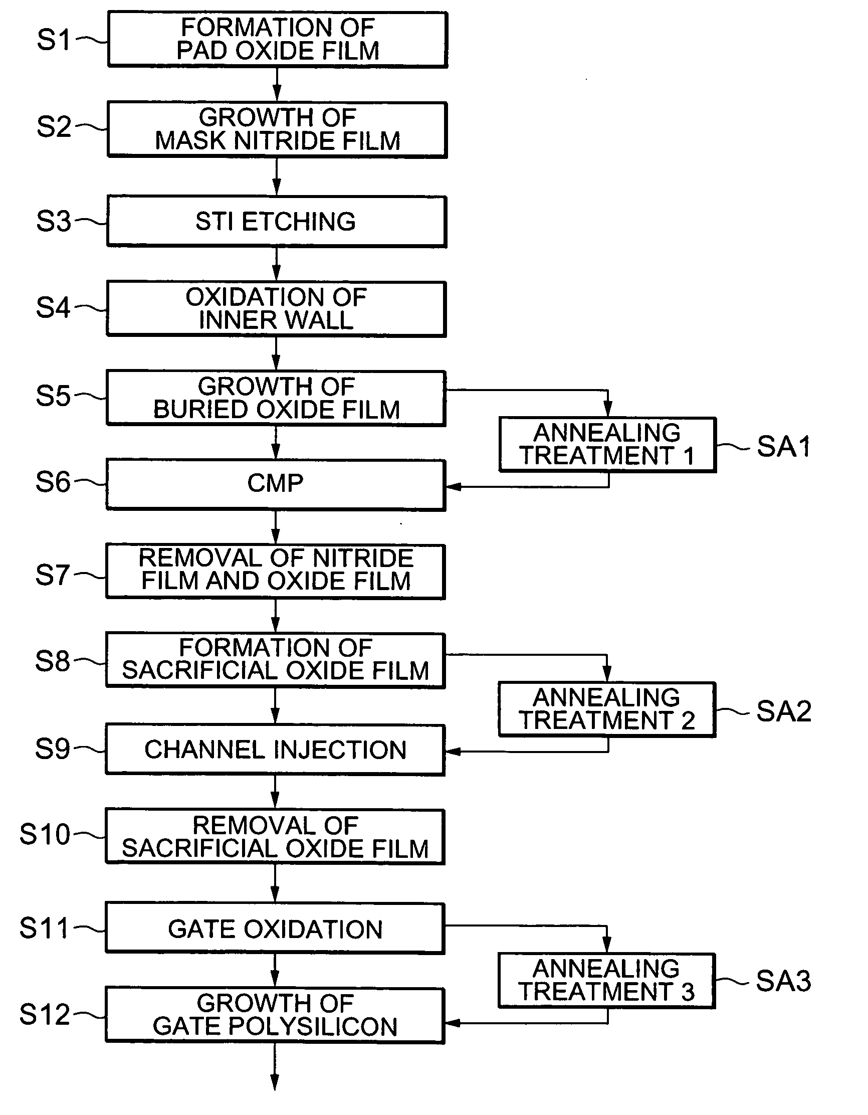
[0028] Methods for producing a semiconductor device according to the present invention will now be described with reference to the drawings.

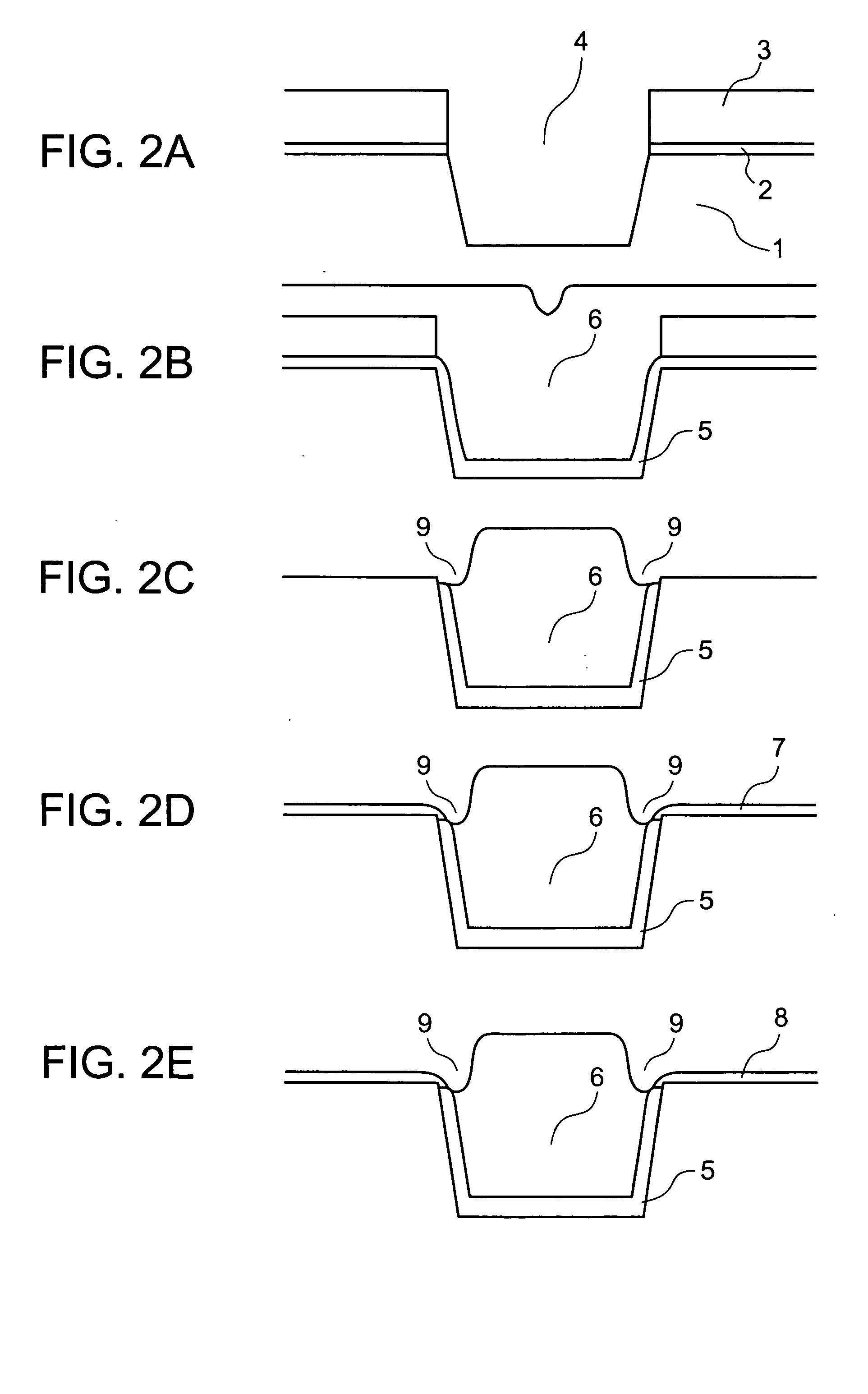
[0029] First, a pad oxide film 2 with a thickness of 9 nm and a nitride film 3 with a thickness of 140 nm are formed on the main surface of a silicon substrate 1, as shown in steps S1 and S2 of FIG. 1 and FIG. 2A. The nitride film 3 and the pad oxide film 2 are then etched by photolithography, and the silicon substrate 1 is etched to form a trench 4, as shown in a step S3 of FIG. 1 and FIG. 2A. The inner wall of the trench 4 is oxidized to form an inner-wall oxide film 5 with a thickness of 20 nm. The trench 4 is then fully filled with a buried oxide film 6, as shown in steps S4 and S5 of FIG. 1 and FIG. 2B.

[0030] The buried oxide film 6 is polished by chemical mechanical polishing (CMP) until the nitride film 3 is exposed, as shown in a step S6 of FIG. 1 and thus a flat surface is formed. The nitride film 3 and the pad oxide film 2 are then r...


PUM


Abstract

A method for producing a semiconductor device includes the steps of forming a trench for device isolation on a silicon substrate; and annealing the silicon substrate in an atmosphere containing a noble gas at any step after the growth of a buried oxide film until the growth of a gate polysilicon.

Description

[0001] This application claims priority to prior Japanese patent application JP 2004-117798, the disclosure of which is incorporated herein by reference. BACKGROUND OF THE INVENTION [0002] The present invention relates to methods for producing semiconductor devices, and particularly relates to a method for producing a semiconductor device without deterioration of device characteristics by improving the reliability of a gate oxide film at the boundary between a trench-isolation region and an active region. [0003] Larger-scale, higher-speed semiconductor devices have increasingly been demanded in recent years. In order to meet the demand, STI (shallow trench isolation) has been used as a method for isolating devices. In STI, an insulating film is buried in a trench to achieve isolation. This method therefore causes no bird's beak in contrast to LOCOS (local oxidation of silicon), and is suitable for achieving high integration. [0004] In STI, however, square STI corners are formed at t...

Claims


Application Information

Patent Timeline
IPC IPC(8): H01L21/28H01L21/76H01L21/316H01L21/324H01L21/762H01L29/78
CPCH01L21/28185H01L21/76224H01L21/28238
Inventor OHASHI, TAKUOSUWA, TAKESHIKUBOTA, TAISHI
Owner ELPIDA MEMORY INC
Why Eureka
Try Eureka