Semiconductor device and method of manufacturing thereof

a technology of semiconductor devices and insulating films, which is applied in the direction of individual semiconductor device testing, pulse technique, emergency protective arrangements for limiting excess voltage/current, etc., can solve the problems of gate insulating film breakdown, high probability of igbt breakdown, and high short-circuit current, so as to eliminate defective elements and enhance reliability of igbt

Inactive Publication Date: 2005-06-09
MITSUBISHI ELECTRIC CORP
View PDF4 Cites 5 Cited by
  • Summary
  • Abstract
  • Description
  • Claims
  • Application Information

AI Technical Summary

Benefits of technology

[0007] It is therefore an object of the present invention to provide a semiconductor device allowing application of a voltage higher than a clamping voltage to a gate insulating film on the way to completion, to thereby eliminate a defective element and enhance reliability of an IGBT.

Problems solved by technology

In the event of a short circuit in a load such as an arm-short, however, high current conductivity results in a higher short-circuit current.
In the event that a parasitic inductance inherent in the gate experiences application of a voltage which is not less than the applied voltage, such a short-circuit current is further increased, thus causing high probability of breakdown of the IGBT.
Further, application of an overvoltage between the gate and the emitter may cause breakdown of a gate insulating film.
However, due to the presence of a clamping element connected between the gate and the emitter, a voltage higher than a clamping voltage cannot be applied between the gate and the emitter.

Method used


Image

  • Semiconductor device and method of manufacturing thereof
  • Semiconductor device and method of manufacturing thereof
  • Semiconductor device and method of manufacturing thereof

Examples


first preferred embodiment

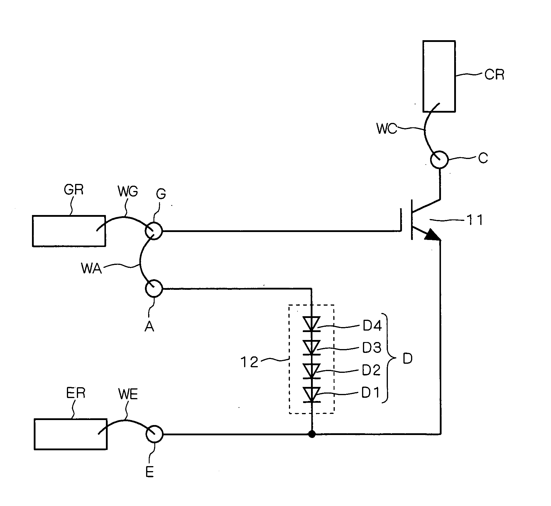
[0016]FIG. 1 shows a semiconductor device according to a first preferred embodiment of the present invention that comprises an IGBT 11 as an exemplary insulated gate semiconductor device. The IGBT 11 and a clamping element 12 are formed on the same semiconductor chip (hereinafter simply referred to as a chip).

[0017] External electrodes GR, CR and ER are wire bonded to a gate terminal (first terminal) G, to a collector terminal C, and to an emitter terminal E formed on the chip, respectively. More particularly, the external electrode GR is connected to the gate terminal G through a bonding wire WG. The external electrode CR is connected to the collector terminal C through a bonding wire WC. The external electrode ER is connected to the emitter terminal E through a bonding wire WE. The IGBT 11 has a gate (control electrode) connected to the gate terminal G, an emitter (first current electrode) connected to the emitter terminal E, and a collector (second current electrode) connected t...

second preferred embodiment

[0029]FIG. 3 shows a semiconductor device according to a second preferred embodiment of the present invention. Those elements corresponding to the components of FIG. 1 are identified with the same reference numerals, and the description thereof will be omitted. The second preferred embodiment comprises a clamping element 31 which characteristically includes a diode DR in addition to the diode D.

[0030] The diode DR has one end connected to the anode terminal A. Another end of the diode DR is connected to the emitter. That is, the diode DR is connected between the anode terminal A and the emitter in inverse-parallel connection to the diode D. The diode DR includes a plurality of diodes connected. In FIG. 3, four diodes including DR1 through DR4 that constitute the diode DR are connected in series anode-to-cathode. The cathode of the diode DR1 is connected to the anode terminal A. The anode of the diode DR4 is connected to the emitter of the IGBT 11. Like in the first preferred embodi...

third preferred embodiment

[0037]FIG. 5 shows a semiconductor device according to a third preferred embodiment of the present invention. Those elements corresponding to the components of FIG. 1 are identified with the same reference numerals, and the description thereof will be omitted. The third preferred embodiment comprises a clamping element 61 having one end connected to the gate, and another end connected to one end of a resistor R2. The resistor R2 has another end connected to the emitter. The clamping element 61 characteristically includes a sensing terminal S. A gate drive circuit 52 is connected through an external electrode not shown to the gate terminal G. The gate drive circuit 52 serves to apply a gate voltage to the gate to actuate the IGBT 11. The sensing terminal S is connected through an external sensing terminal not shown to the gate drive circuit 52.

[0038] The clamping element 61 comprises the diodes D and DR. The diode D includes a plurality of diodes connected. In FIG. 5, four diodes in...


PUM


Abstract

The gate of an IGBT is connected to a gate terminal. One end of a clamping element is connected to an anode terminal. A voltage higher than a clamping voltage is applied between the gate and the emitter, to thereby test the dielectric breakdown voltage of a gate insulating film of the IGBT. The IGBT is eliminated which has a gate insulating film at a dielectric breakdown voltage failing to fall within its proper distribution range. Thereafter, a gate terminal and an anode terminal are wire bonded in the normal IGBT.

Description

BACKGROUND OF THE INVENTION [0001] 1. Field of the Invention [0002] The present invention relates to a semiconductor device and more particularly, it relates to a semiconductor device comprising an insulated gate semiconductor device and a clamping element for providing clamp of a gate-emitter voltage of the insulated gate semiconductor device. [0003] 2. Description of the Background Art [0004] Insulated gate semiconductor devices such as IGBTs and power MOSFETs are widely used for power conversion. The IGBTs feature high speed operation of MOSFETs and low on-stage voltage of bipolar transistors, and hence, are especially in wide use in power converters such as inverters. [0005] The IGBT is equivalent circuit to a combination of an MOSFET and a bipolar transistor. For lower loss of the IGBT, there is a trend toward higher current conductivity of the MOSFET by means of scaledown, for example. In the event of a short circuit in a load such as an arm-short, however, high current conduc...

Claims


Application Information

Patent Timeline
Patent Type & Authority Applications(United States)
IPC IPC(8): G01R31/26H01L21/822H01L27/04H01L29/78H03K17/0812
CPCH01L24/06H01L24/49H01L2924/1305H01L2924/30107H01L2924/13055H01L2924/13091H01L2924/01068H01L2924/01033H01L2924/01024H01L2924/01023H01L2924/01021H01L2924/00014H03K17/08128H01L2924/01082H01L2924/01006H01L2224/05599H01L2224/48091H01L2224/4813H01L2224/4911H01L2224/85399H01L2924/01004H01L2224/45099H01L2924/00H01L24/48H01L2924/12035H01L2924/12036H01L29/6609H01L29/66325H01L29/802
Inventor TADOKORO, CHIHIROTOMOMATSU, YOSHIFUMI
Owner MITSUBISHI ELECTRIC CORP
Why Eureka
Try Eureka