Low cost high-pressure sensor
a high-pressure sensor, low-cost technology, applied in the direction of fluid pressure measurement, variable capacitors, instruments, etc., can solve the problems of inconvenient mass production of sensors, high manufacturing cost of these sensors, and inability to meet the needs of mass production
- Summary
- Abstract
- Description
- Claims
- Application Information
AI Technical Summary
Benefits of technology
Problems solved by technology
Method used
Image
Examples
example 1
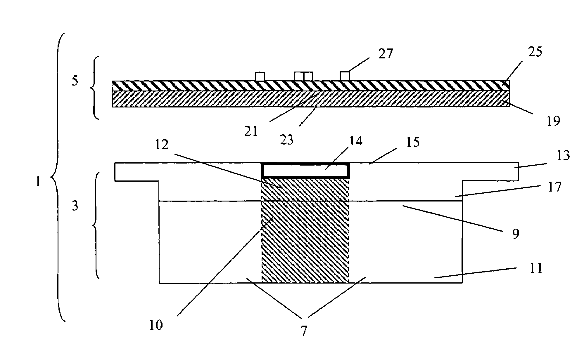
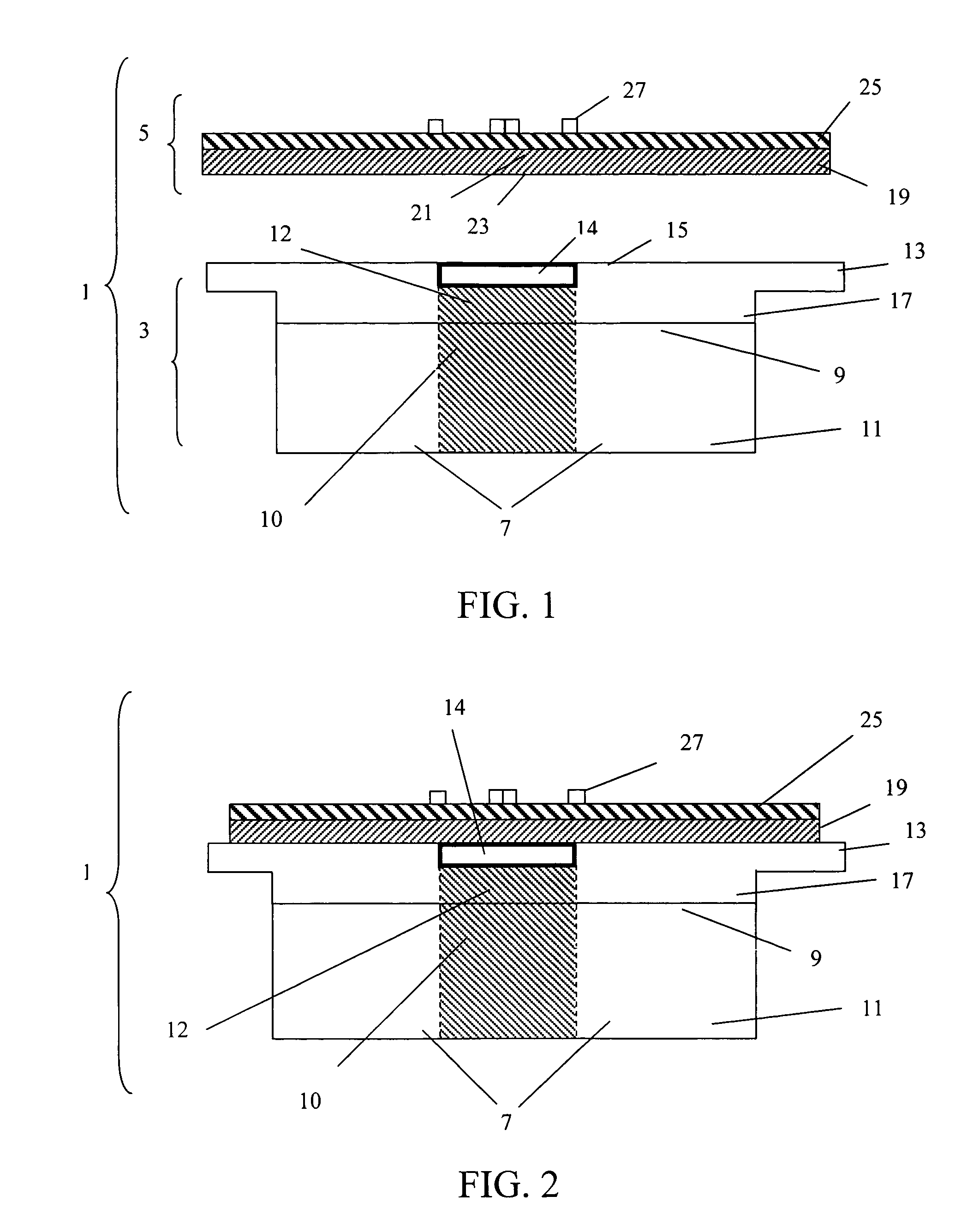
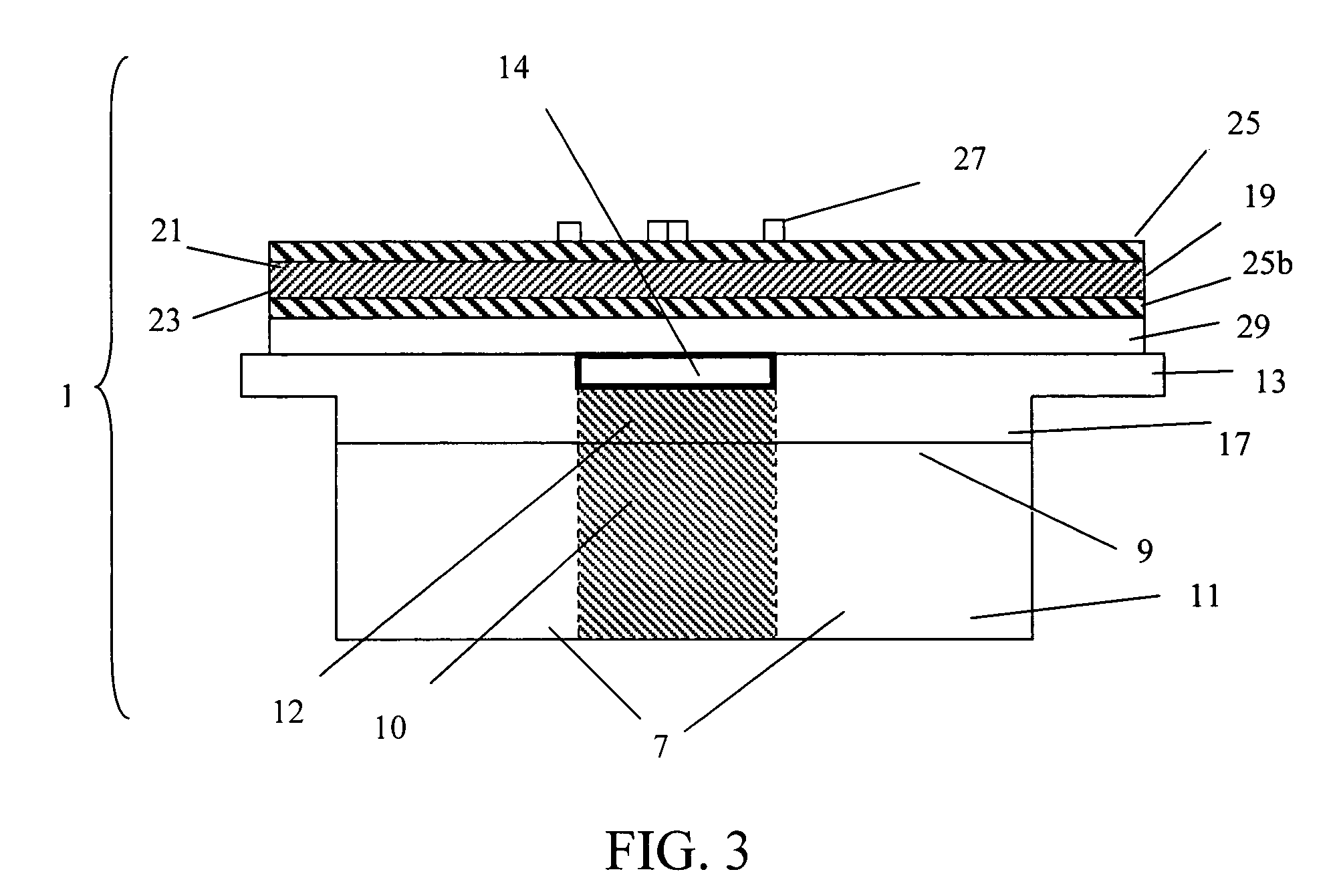
[0064]A circular, flat disc of 430 stainless steel is machined to have a diameter of 0.5 mm and a thickness of 0.1 mm, and is washed in detergent. A ceramic dielectric paste comprising alumina is screen printed onto an upper surface of the disc. The ceramic paste is dried on the disc in an oven for 10-15 minutes at 150° C. The dried paste is then fired on the disc for 60-90 minutes at 850-950° C. to form a ceramic coating having a thickness of about 0.05 mm. Piezoresistive elements are then formed on the ceramic coating by first screen printing a conductive gold paste onto the ceramic coating. The conductive paste is then dried on the ceramic coating in an oven for 10-15 minutes at 150° C. The conductive paste is then fired on the ceramic coating for 60-90 minutes at 850° C. to form a conductive layer having a thickness of about 0.01 mm. A resistor paste is then screen printed onto the conductive layer. The resistor paste is then dried on the conductive layer in an oven for 10-15 mi...
example 2
[0066]A circular, flat ceramic disc comprising alumina is formed, having a diameter of 0.5 mm and a thickness of 0.1 mm, and is washed in detergent. Piezoresistive elements are then formed on the ceramic coating by first screen printing a conductive gold paste onto the ceramic coating. The conductive paste is then dried on the ceramic coating in an oven for 10-15 minutes at 150° C. The conductive paste is then fired on the ceramic coating for 60-90 minutes at 850° C. to form a conductive layer having a thickness of about 10 microns. A resistor paste is then screen printed onto the conductive layer. The resistor paste is then dried on the conductive layer in an oven for 10-15 minutes at 150° C. The resistor paste is then fired on the conductive layer for 60-90 minutes at 850° C. to form a resistor layer having at thickness of about 0.02 mm.
[0067]Separately, a 316 stainless steel pressure port is welded to a 316 stainless steel diaphragm assembly. The diaphragm assembly includes a cen...
example 3
[0068]Example 1 is repeated except that after firing the resistor paste, an overglaze glass sealant paste is screen printed onto the resistor layer and dried in an oven for 10-15 minutes at 150° C. The overglaze glass sealant paste is then fired for 30-60 minutes at 500-700° C. to form an overglaze glass sealant layer having a thickness of 0.01-0.02 mm.
PUM
| Property | Measurement | Unit |
|---|---|---|
| thickness | aaaaa | aaaaa |
| diameter | aaaaa | aaaaa |
| thickness | aaaaa | aaaaa |
Abstract
Description
Claims
Application Information


