Integrated imager circuit comprising a monolithic array of single photon avalanche diodes

a monolithic array and imager technology, applied in the field of integrated imager circuits, can solve the problems of power dissipation, speed requirement on the sensor, and power dissipation, and achieve the effects of tight speed and accuracy specifications, low power dissipation, and high sensitivity

Active Publication Date: 2007-08-28
ECOLE POLYTECHNIQUE FEDERALE DE LAUSANNE (EPFL)
View PDF7 Cites 123 Cited by
  • Summary
  • Abstract
  • Description
  • Claims
  • Application Information

AI Technical Summary

Benefits of technology

[0019]This has the advantage that a single circuit can be used for capturing 2D and 3D data, i.e. brightness and depth. Furthermore, as SPADs operating in 2D and 3D mode are both available on the circuit, brightness and depth measurement can be performed simultaneously, using light from the same light pulse.
[0020]The readouts circuits are preferably at least partially integrated on the same chip, thus providing a compact, inexpensive imaging 2D and 3D circuit.
[0021]To reach millimetric accuracies, an array of highly sensitive, ultra-low jitter CMOS detectors capable of detecting a single photon are preferably used. The scene may be illuminated by using a cone of low power pulsed laser light, thus no mechanical scanning devices or expensive optical equipment is required.
[0022]In a preferred embodiment, the SPADs are CMOS-implemented and operated in the Geiger mode. CMOS implementation allows for an inexpensive integration and better scalability.
[0029]In an embodiment, the solid-state 3D imager circuit of the invention is based on the pulsed type TOF (time of flight) method. The sensor, implemented in standard CMOS technology, consists of an array of single photon avalanche diodes (SPADs), capable of performing a great amount, such as 1024 or more, of independent distance measurements, and an external or integrated low-cost CMOS time discriminator (for example TDCs). The scene is illuminated using a single intentionally uncollimated laser beam to create a cone of light that synchronously reaches every point of the surface. This technique eliminates the need for a mechanical device to scan the entire scene. Moreover, due to the sensor's high sensitivity, inexpensive laser sources with milliwatt peak power can be used for ranges up to several meters.
[0030]A time precision of a few tens of picoseconds is made possible by the jitter properties of SPADs when operating in Geiger mode. A 3D camera system of the invention is capable of characterizing the optical field by mapping both the depth of the scene as well as the intensity of the light reflected by it. Extremely tight speed and accuracy specifications are met, while keeping power dissipation to a minimum thanks to the inherent simplicity of the sensor design. Moreover, due to the reduced power of the laser source, it is possible to guarantee strict eye safety operation of the system even with a duty cycle of 100%.

Problems solved by technology

The main disadvantages of such systems are the speed requirement on the sensor (usually a conventional CMOS or CCD camera), power dissipation, and a somewhat limited precision.
However, interferometers are usually bulky and very expensive.
However, relatively powerful laser or LED sources are still required and accuracy is limited by the speed at which the sensor can be clocked.
If conventional detectors were to be used, time discrimination could only be achieved through highly sophisticated detectors and / or very powerful laser sources.
The sensor is not CMOS compatible and necessitates a complex technology, expensive and hard to integrate on a monolithic chip.
Usage of two different chips, and wire-bonding of the chips, makes the fabrication of very high resolution chip expensive.
Multiple technologies could be combined on a single chip; however this is also an expensive proposition.
Moreover, prior art tri-dimensional imaging circuits based on diodes operating in Geiger-mode only deliver a monochromatic depth map for indicating the distance between the circuit and each point of the scene.
Lack of information regarding the brightness or color of the scene limits the value of those circuits.
This solution is thus hardly scalable and poorly adapted to arrays comprising tens or even hundreds of SPADs, as required by modern imagers.
Although this document does suggest to use the sensor in 2D mode, it does not disclose which parameters of the scene are captured in 2D mode, and does not adequately describe any 2D or 3D readout circuit in the manner necessary for one to design or manufacture the circuit.

Method used


Image

  • Integrated imager circuit comprising a monolithic array of single photon avalanche diodes
  • Integrated imager circuit comprising a monolithic array of single photon avalanche diodes
  • Integrated imager circuit comprising a monolithic array of single photon avalanche diodes

Examples


Embodiment Construction

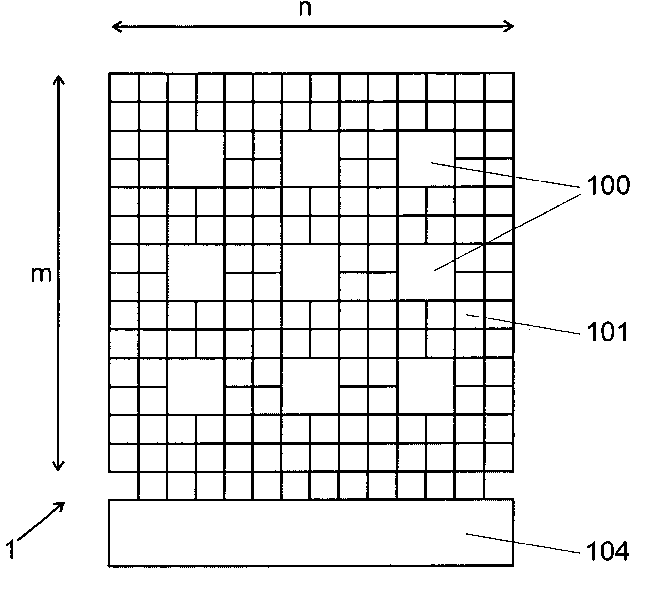
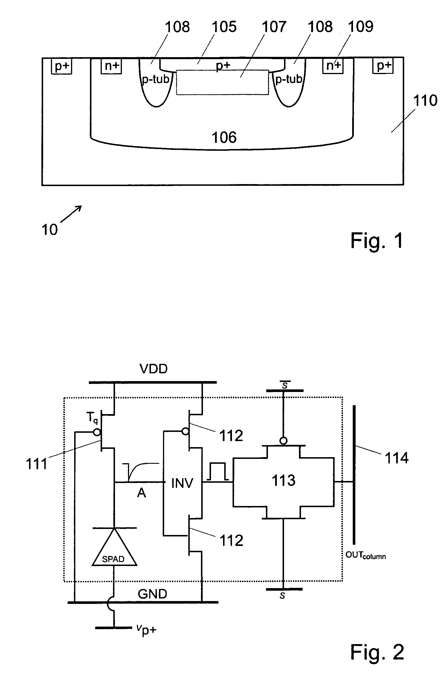
[0040]FIGS. 1 and 3 illustrate a CMOS implemented SPAD according to the invention. A SPAD is a p-n junction biased above breakdown voltage Vbd by an excess voltage Ve of a few volts. Operated in the so-called Geiger mode, avalanche photodiodes can react on single photons. A primary carrier resulting from the absorption of a photon may generate a nearly-infinite number of secondary electron-hole pairs by impact ionization.

[0041]The SPAD illustrated in FIG. 1 comprises a p / n junction 107 between a p+ region 105 (anode) and a deep n tub (n well) 106. A second junction exists between the deep n tub and the p substrate 110. The depth of those junctions and the doping profile of the different regions may be adapted to the wavelength one wants to detect.

[0042]The upper p+ / deep n-tub junction 107 provides the multiplication region where the Geiger breakdown (the avalanche) occurs, regularly triggered by photons, possibly by simple photons

[0043]For a SPAD to operate in avalanche mode, the up...


PUM


Abstract

An integrated imager circuit having a monolithic array of single photon avalanche diodes (SPADs) for capturing an image of a scene when said scene is hit by an optical pulse. The array has a plurality of SPADs connected to 2D readout circuits which determines the intensity of the light reflected by the scene by counting the number of photons received by the SPADs during a period of time. A plurality of SPADs connected to 3D readout circuits determines the distance to the scene by determining the elapsed time between the emission of each pulse and reception of the corresponding reflected photons.

Description

[0001]The present application claims priority of U.S. provisional patent 60 / 652,010, filed on Feb. 14, 2005.[0002]The present application also incorporates by reference the content of U.S. utility patent application U.S. Ser. No. 11 / 290,831, filed on Dec. 1, 2005, and of U.S. provisional patent application U.S. 60 / 652,010, filed on Feb. 14, 2005.FIELD OF THE INVENTION[0003]The present invention concerns an integrated imager circuit comprising a monolithic array of single photon avalanche diodes, and an imaging system using such a circuit for reconstructing the brightness and / or the depth map of an arbitrary scene.DESCRIPTION OF RELATED ART[0004]A number of new and potentially high volume applications require fast and precise depth map evaluation. These applications include face recognition systems, virtual keyboards, object and person monitoring, land and sea surveyors, virtual reality games, non-ionising medical tomographic imagers, stage and choreography analysis tools, etc. Speed...

Claims


Application Information

Patent Timeline
Patent Type & Authority Patents(United States)
IPC IPC(8): H01L31/00H01L27/00
CPCH01L27/14647H01L31/107
Inventor NICLASS, CRISTIANOCHARBON, EDOARDOBESSE, PIERRE-ANDREROCHAS, ALEXIS
Owner ECOLE POLYTECHNIQUE FEDERALE DE LAUSANNE (EPFL)
Why Eureka
Try Eureka