Ion-sensitive structure and method for producing the same

a technology of ion-sensitive structures and capacitance measurements, applied in the field of ion-sensitive structures, can solve the problems of insufficient knowledge of the disadvantages of glass electrodes with respect to semiconductor sensors, inability to obtain electrical long-term stability and accuracy, and inability to read out structures only via capacitance measurement, etc., to achieve the effect of improving stability and sensitivity, low cross-sensitivity, and minimal dri

Active Publication Date: 2016-09-22
FRAUNHOFER GESELLSCHAFT ZUR FOERDERUNG DER ANGEWANDTEN FORSCHUNG EV
View PDF6 Cites 0 Cited by
  • Summary
  • Abstract
  • Description
  • Claims
  • Application Information

AI Technical Summary

Benefits of technology

[0022]By means of the inventive ion-sensitive structure, an improved stability and sensitivity with regard to the ions to be detected is obtained with respect to previously used metal oxides, wherein further low cross-sensitivity and minimum drift is obtained at good long-term stability of a sensor comprising the ion-sensitive structure. This is, for example, obtained since doping of the metal oxide material results in a reduction of structural defects in the layer in comparison to a number of structural defects of the metal oxide material without presence of a dopant.

Problems solved by technology

All other semiconductor / insulator combinations are mostly electrically not as stable or the necessitated electrical long term stability and accuracy can only be obtained with increased effort.
However, the disadvantages of glass electrodes with respect to semiconductor sensors are sufficiently known, as well as how the EIS structure is used for analysis.
However, such a structure can only be read out via capacitance measurement necessitating a measurement cell with a Faraday cage.
Thus, the same are chemically less stable and more light-sensitive than their crystalline counterparts in bulk chemistry and are subject to planar etching at increased temperature in corrosive media.
The weaknesses of these layers are the grain boundaries of the crystallites, in particular the vertical ones allowing pore etching and consequences of sub-etching at increased temperature in aggressive media.
Multilayered amorphous metal oxides of different substances are chemically more stable than simple ones, but the problems accompanying amorphous structures could not be satisfactorily solved.
The crystallizations of these multilayers of different metal oxide layers are, as can be expected, again chemically more stable, but the interfaces between the substance types result in typical interface problems.
These are poor reproducibility of the flat band voltage and so-called charge trapping.
The deposition of metals with subsequent thermal oxidation [12] results, for kinetical reasons, in poor quality of the semiconductor / insulator combination, such as Si / SiO2, since the metal has a reducing effect on an applied insulator (e.g., SiO2) and thereby partly removes the oxygen from the insulator layer.
This results in fixed charges in the gate insulator causing operating point shifts of the sensor and drifts by trapping processes.
The trapping processes result in leakage currents which affect the chemical stability of the whole insulator stack.
The same responds to the temperings necessitated for stabilization and compression with extensive anisotropic thermal expansions which can lead to cracks in the layer at topology edges.
Even when HfO2 is deposited in one or several thin amorphous layers and tempered with Ta2O5, the charges at the interfaces and in the HfO2 layer itself are only difficult to control.

Method used


Image

  • Ion-sensitive structure and method for producing the same
  • Ion-sensitive structure and method for producing the same
  • Ion-sensitive structure and method for producing the same

Examples


Embodiment Construction

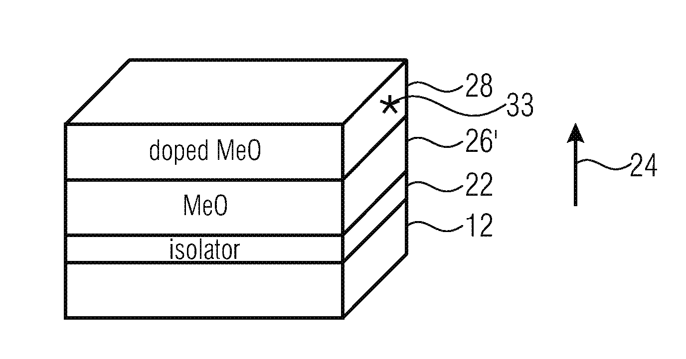
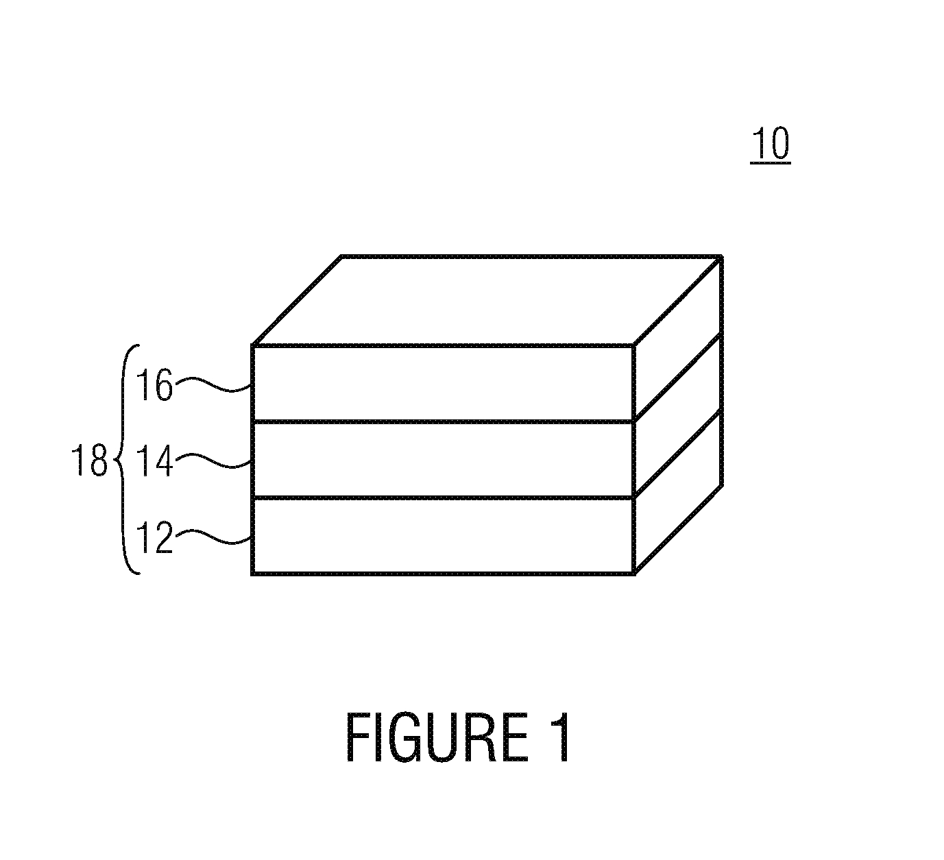
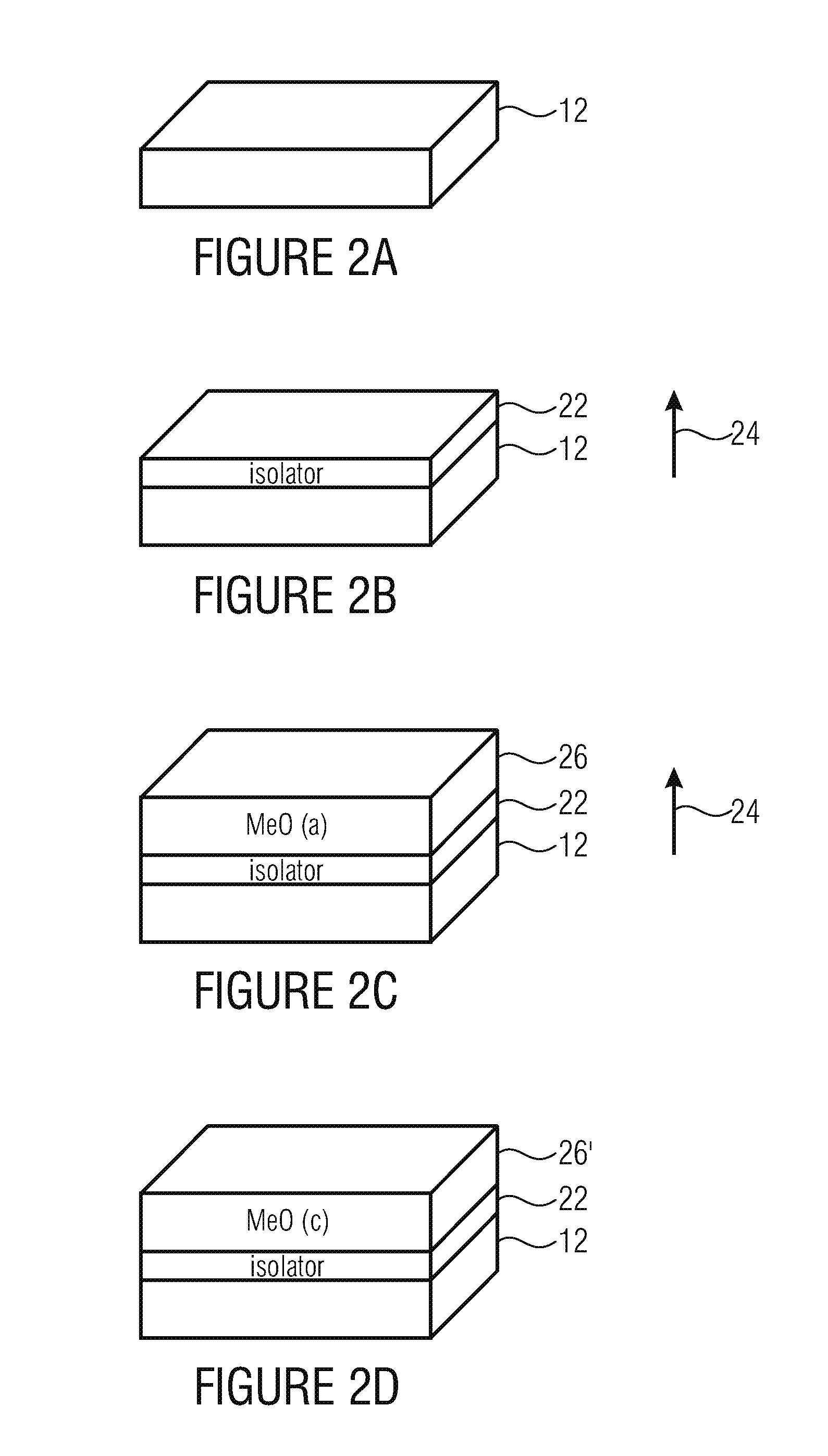
[0049]Before embodiments of the present invention will be discussed in detail based on the drawings, it should be noted that identical, functionally equal or similar elements, object and / or structures are provided with the same reference numbers in the different figures, such that the description of these elements represented in different embodiments is inter-exchangeable or can be applied to one another.

[0050]FIG. 1 shows a schematic perspective view of an ion-sensitive structure 10 according to an embodiment. The ion-sensitive structure 10 includes a semiconductor structure 12. The semiconductor structure 12 can, for example, be a processed semiconductor substrate. The processed semiconductor substrate can, for example, be a semiconductor substrate suitable for a transistor, which comprises npn or pnp structures.

[0051]A doped intermediate layer 14 is disposed on a main side of the semiconductor structure 12. The doped intermediate layer 14 includes a doping material and a metal ox...


PUM

PropertyMeasurementUnit
thicknessaaaaaaaaaa
thicknessaaaaaaaaaa
thicknessaaaaaaaaaa

Abstract

An ion-sensitive structure includes a semiconductor structure and a layer stack disposed on the semiconductor structure having a doped intermediate layer including a doping material and a first metal oxide material. The semiconductor structure is configured to change an electric characteristic based on a contact of the ion-sensitive structure with an electrolyte including ions.

Description

CROSS-REFERENCE TO RELATED APPLICATIONS[0001]This application claims priority from German Patent Application No. 102015204921.3, which was filed on Mar. 18, 2015, and is incorporated herein in its entirety by reference.BACKGROUND OF THE INVENTION[0002]The present invention relates generally to an ion-sensitive structure and to a method for producing the same. The ion-sensitive structures can be used, for example, in ion-sensitive field effect transistors (ISFETs), ion-sensitive, capacitively readable EIS sensors or LAPS sensors. In particular, the present invention relates to a chemically stable multilayered structure having doped zones.[0003]In microsystem technology of semiconductor technology, chemically stable surfaces are necessitated as chemical protection for sensor or actuator surfaces for sensors and actuators in the different fields of application, for example environmental technology, process monitoring, food technology as well as biochemistry or medical technology. When ...

Claims


Application Information

Patent Timeline
Patent Type & Authority Applications(United States)
IPC IPC(8): G01N27/414
CPCG01N27/4148G01N27/129G01N27/414G01N27/333
Inventor KURTH, EBERHARDKUNATH, CHRISTIANSCHENK, HARALD
Owner FRAUNHOFER GESELLSCHAFT ZUR FOERDERUNG DER ANGEWANDTEN FORSCHUNG EV
Why Eureka
Try Eureka