Power-on reset circuit

a power-on reset and circuit technology, applied in the direction of pulse automatic control, pulse technique, electronic switching, etc., can solve the problems of power-on reset circuit, drawback of flip-flop use, and inability to minify the square measure of the entire lsi

Inactive Publication Date: 2007-08-28
PANASONIC CORP
View PDF11 Cites 2 Cited by
  • Summary
  • Abstract
  • Description
  • Claims
  • Application Information

AI Technical Summary

Benefits of technology

[0012]The present invention aims to provide a power-on reset circuit in which power-on reset signal surely becomes active regardless of the rise time of power supply voltage, and which can be well-integrated.
[0017]Since the circuit of the present invention is composed of transistors only, the power-on reset circuit that is inexpensive and is well-integrated can be provided.
[0025]The power-on reset circuit of the present invention can set the time width of a power-on reset signal according to the capacity of the capacitor and / or the resistance value of the second resistor composing the pulse generating circuit.
[0029]According to the present invention, an advantageous effect capable of realizing a power-on reset circuit which surely generates a power-on reset signal regardless of the rise time of power supply voltage, can be obtained.
[0030]According to the present invention, an advantageous effect capable of realizing a power-on reset circuit which surely generates a power-on reset signal regardless of variety of the rise time of power supply voltage, and which can be integrated into an IC, can be obtained.

Problems solved by technology

Furthermore, the power-on reset circuit of the conventional art has a problem in which square measure of the entire LSI cannot be minified since the capacitor 10 is included.
However, since the flip-flop occupies a large area in the LSI, the use of the flip-flop was a drawback in the integration of the power-on reset circuit.
And there has been a problem of dispensing with the flip-flop.

Method used


Image

  • Power-on reset circuit
  • Power-on reset circuit
  • Power-on reset circuit

Examples


first embodiment

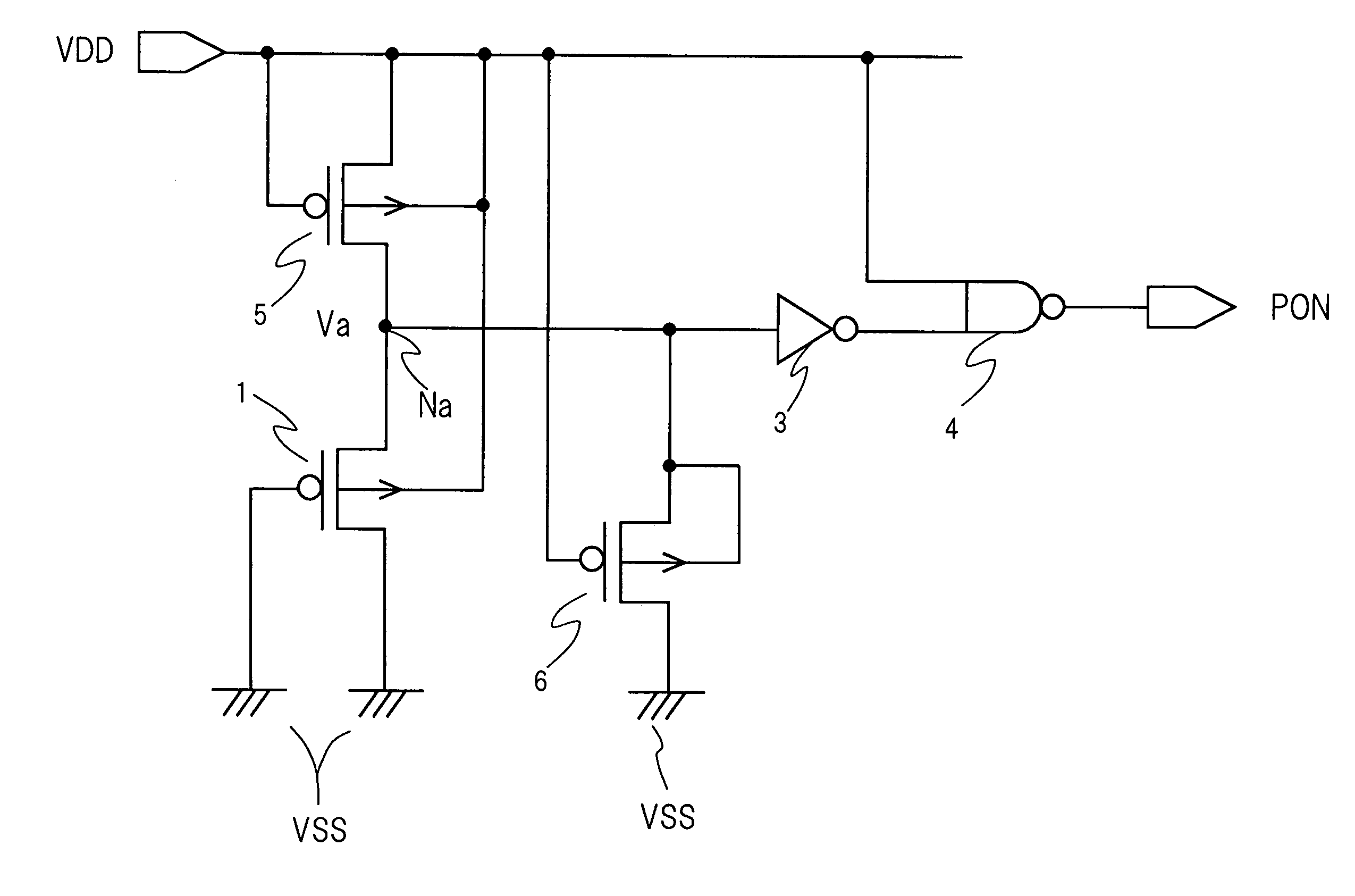
[0046]The power-on reset circuit in accordance with the first embodiment is comprised of a first p-channel MOS transistor 1, a first resistor 2, a first inverter 3 and a NAND circuit 4. The first resistor 2 and the first p-channel MOS transistor 1 is connected in series between a power supply potential VDD and a ground potential VSS. The gate and the drain of the first p-channel MOS transistor 1 are connected to a ground potential VSS, and a substrate is connected to the power supply potential VDD. “Na” is a connecting point of the first resistor 2 with the source of the first p-channel MOS transistor 1.

[0047]The source of the first p-channel MOS transistor 1 is connected to the input terminal of the first inverter 3. The power supply potential VDD and the output terminal of the first inverter 3 are connected to the two input terminals of the NAND circuit 4 respectively, and the output terminal of NAND circuit 4 is connected to a power-on reset signal output terminal. The output ter...

third embodiment

[0059]In the power-on reset circuit in accordance with the third embodiment, when the power supply potential VDD drops drastically from “Ve” to zero V, the potential Va of the connecting point Na only drops to “−Vd” wherein pn junction voltage between the drain and the substrate of the third p-channel MOS transistor 6 is assumed as Vd. Therefore, the power-on reset signal PON can be generated normally even during the recovery of power supply potential.

>

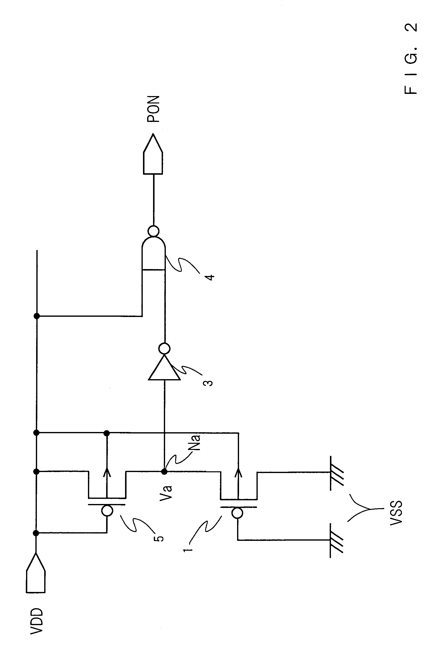
[0060]FIG. 6 is a circuit diagram of a power-on reset circuit in accordance with the fourth embodiment of the present invention. The power-on reset circuit in accordance with the fourth embodiment further comprises a first n-channel MOS transistor 7 added to the power-on reset circuit in accordance with the second embodiment. In the first n-channel MOS transistor 7, the gate, the drain and a substrate are connected to a ground potential VSS, and the source is connected to a connecting point Na. Other configurations are same as those o...

fourth embodiment

[0061]Operations in the case where power supply potential VDD drops drastically from “Ve” to zero V and then recovers soon (instantaneous power interruption), after the power is turned on, the power-on reset signal PON becomes active and then later becomes inactive, will be described. In the power-on reset circuit in accordance with the fourth embodiment, when the power supply potential VDD drops drastically from “Ve” to zero V, the potential Va of the connecting point Na only drops to “−Vd” wherein pn junction voltage between the drain and the substrate of the first n-channel MOS transistor 7 is assumed as “Vd”. Therefore, the power-on reset signal PON can be generated normally even during the recovery of power supply potential.

[0062]The power-on reset circuit in accordance with the fourth embodiment exerts the same effect as the power-on reset circuit in accordance with the third embodiment.

>

[0063]A power-on reset circuit in accordance with the fifth embodiment of the present inve...


PUM


Abstract

A power-on reset circuit of the present invention comprises: a first p-channel MOS transistor having the gate and the drain which are grounded and having a substrate which is connected to a power supply; a first resistor which is inserted and connected between the above-mentioned power supply and the source of the above-mentioned first p-channel MOS transistor; a first inverter having an input terminal which is connected to the source of the first p-channel MOS transistor; and a power-on reset signal output terminal which is connected to an output terminal of the first inverter.

Description

TECHNICAL FIELD[0001]The present invention relates to a power-on reset circuit.[0002]A power-on reset circuit is incorporated on a digital system having a need to reset the system and initialize data immediately after power is turned on.[0003]The power-on reset circuit of the conventional art will be described with reference to FIG. 9, FIG. 10 and FIG. 11. The power-on reset circuit of the conventional art is shown in FIG. 9. In the power-on reset circuit of the conventional art, a resistor 30 and a capacitor 10 are series-connected between a power supply potential VDD and a ground potential VSS. An input terminal of an inverter 40 is connected to a connecting point Na between the resistor 30 and the capacitor 10. The two input terminals of an AND circuit 20 are connected to an output terminal of the inverter 40 and the power supply potential VDD, respectively, and an output terminal of the AND circuit 20 is connected to a power-on reset signal output terminal. The output terminal o...

Claims


Application Information

Patent Timeline
Patent Type & Authority Patents(United States)
IPC IPC(8): H03L7/00H03K17/22
CPCH03K17/223
Inventor KINUGASA, NORIHIDENIRASAWA, YOSHIOHAMAGUCHI, HIDEO
Owner PANASONIC CORP
Why Eureka
Try Eureka