Semiconductor memory device with hierarchical I/O line architecture

a memory device and hierarchical technology, applied in the field of synchronous semiconductor memory devices, can solve the problems of increasing the operating current, increasing the chip size, and increasing the operating current of the memory device, and achieve the effect of reducing the operating curren

Active Publication Date: 2007-09-04
LONGITUDE LICENSING LTD
View PDF10 Cites 10 Cited by
  • Summary
  • Abstract
  • Description
  • Claims
  • Application Information

AI Technical Summary

Benefits of technology

[0044]Therefore, an object of the present invention is to provide a semiconductor memory device with a reduced operating current.
[0045]Another object of the present invention is to provide a semiconductor memory device superior in the stability of high-speed (or high-frequency) operation.

Problems solved by technology

These two trends are undesirably accompanied by the increase in the chip size.
One drawback of the above-described operation is the increase in the operating current due to frequent switching of the I / O switch timing signals SWIO_A and SWIO_B.
This undesirably increases the operating current of the memory device.
This would interfere with the implementation of high-speed and high-frequency operations.

Method used


Image

  • Semiconductor memory device with hierarchical I/O line architecture
  • Semiconductor memory device with hierarchical I/O line architecture
  • Semiconductor memory device with hierarchical I/O line architecture

Examples


first embodiment

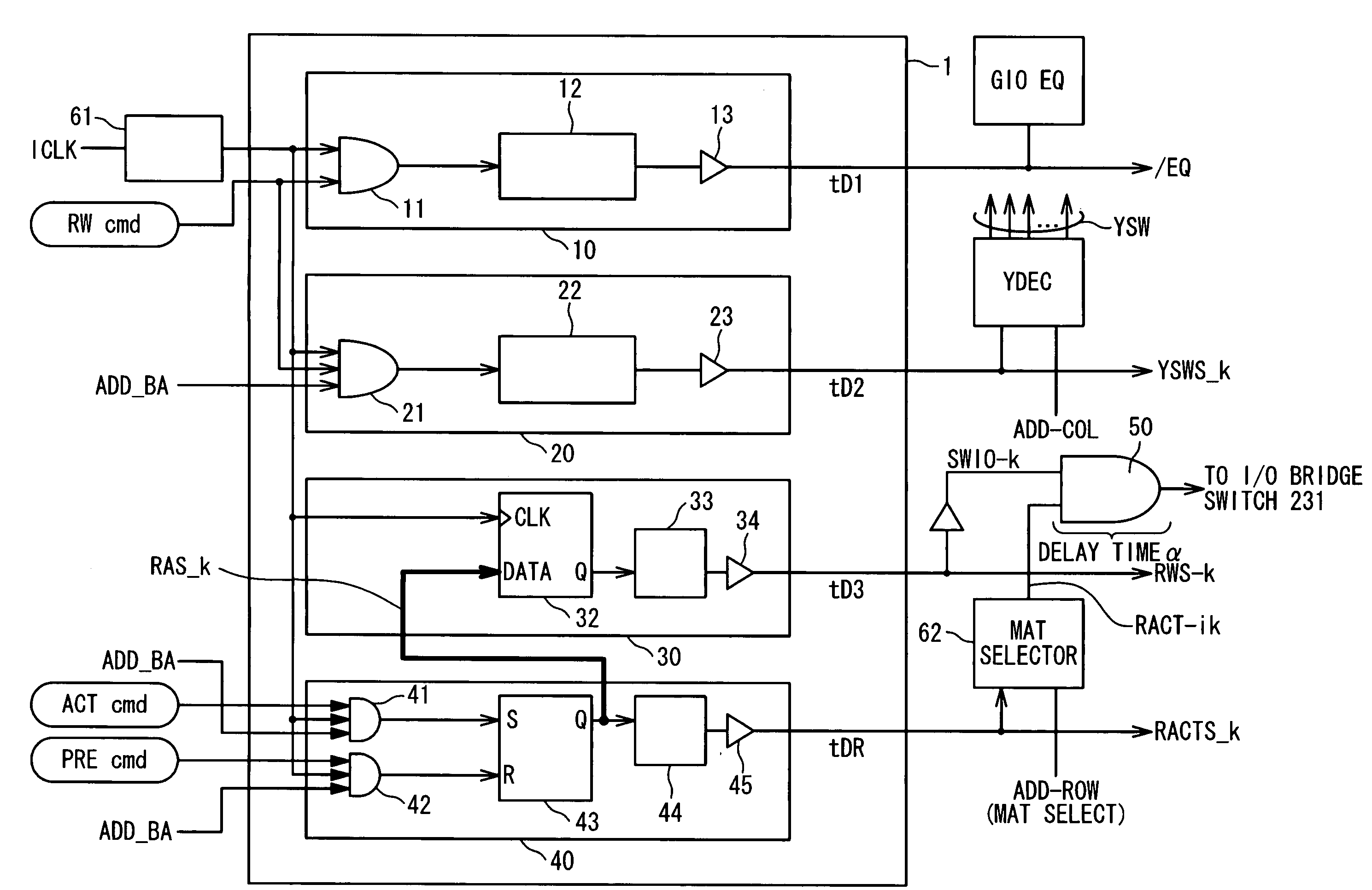
[0076]FIG. 5 is a block diagram illustrating an exemplary structure of the timing control circuit 1 in a first embodiment of the present invention. The timing control circuit 1 receives an internal clock ICLK through a delay circuit 61. The timing of the received internal clock ICLK is adjusted by the delay circuit 61 so as to satisfy timing requirements, such as setup and hold times with respect to input data, including bank addresses. The timing control circuit 1 includes first to fourth logic circuits 10, 20, 30, and 40.

[0077]The first logic circuit 10 generates the GIO equalization timing signal / EQ in synchronization with the internal clock signal ICLK. Specifically, the first logic circuit 10 includes an AND gate 11, a delay circuit 12, and a buffer 13. The AND gate 11 receives the internal clock ICLK and the RWcmd signal on the inputs thereof, and outputs the results of the logical AND operation to the delay circuit 12. The output signal of the AND gate 11 is transferred to t...

second embodiment

[0116]FIG. 8 is a block diagram showing a structure of a timing control circuit 1′ in a second embodiment of the present invention. The timing control circuit 1′ includes the first logic circuit 10, the second logic circuit 20, a third logic circuit 70, and a fourth logic circuit 80. It should be noted that the same elements are denoted by the same numerals in FIGS. 5 and 8. The third and fourth logic circuits 70 and 80 within the timing control circuit 1′ are different in the structure and operation from the third and fourth logic circuits 30 and 40 within the timing control circuit 1 shown in FIG. 5.

[0117]The third logic circuit 70 generates the column activation signals RWS_A and RWS B; it should be noted that FIG. 8 only illustrates the circuitry associated with one of the column activation signal RWS_A and RWS_B, and the symbol “RWS_k” collectively denotes the column activation signal RWS_A and RWS_B. The third logic circuit 130 includes a pair of AND gates 71 and 72, a SR flip...


PUM


Abstract

A semiconductor memory device is composed of a plurality of banks each including a plurality of sub-arrays arranged in rows and columns; global I / O lines shared by the plurality of banks; local I / O lines disposed for every a number of sub-arrays within each of the plurality of banks; I / O switch control circuits responsive to respective I / O switch timing signals for establishing connections between the global I / O lines and the local I / O lines within each of the plurality of banks; and a timing control circuit. The timing control circuit controls the I / O switch timing signals that each I / O switch timing signal remains activated until associated one of the plurality of banks gets out of a row active state after once the each I / O switch timing signal is activated.

Description

BACKGROUND OF THE INVENTION[0001]1. Field of the Invention[0002]The present invention relates to a semiconductor memory device, and in particular, to a synchronous semiconductor memory device.[0003]2. Description of the Related Art[0004]A semiconductor memory device, such as dynamic random access memories (DRAMs), often adopts multiple-bank architecture. The multiple-bank architecture allows virtually eliminating the RAS precharge time (often referred to as tRP) by alternately or sequentially activating multiple banks, and thereby effectively reduces the access time and cycle time. One recent trend is the increase in the number of banks within a semiconductor memory device for achieving the increased memory capacity and improved random access performance; the number of banks within a DRAM is typically increased up to eight or more. Another recent trend is the increase in the bit width within a semiconductor memory device, which is accompanied by the increase in the number of interna...

Claims


Application Information

Patent Timeline
Patent Type & Authority Patents(United States)
IPC IPC(8): G11C7/00
CPCG11C11/4076G11C11/4097G11C2207/002
Inventor MOCHIDA, YOSHIFUMI
Owner LONGITUDE LICENSING LTD
Why Eureka
Try Eureka