
Semiconductor memory device, and signal line layout structure thereof

a semiconductor memory and signal line technology, applied in the direction of information storage, static storage, digital storage, etc., can solve the problems of weakening of power supply to the memory device, achieve the effect of reducing page size, retaining data input/output bandwidth, and increasing the area of the semiconductor memory devi

Active Publication Date: 2019-06-11
SK HYNIX INC
View PDF8 Cites 0 Cited by
  • Summary
  • Abstract
  • Description
  • Claims
  • Application Information

AI Technical Summary

Benefits of technology

This approach allows for reduced operating current while maintaining data bandwidth, optimizing area usage and power efficiency by selectively driving bit line sense amplifiers and dividing data transmission lines.

Problems solved by technology

On other hand, if the page size is reduced, the area of the memory device or the number of data lines is accordingly increased so that supply of power to the memory device may weaken.

Method used


Image

  • Semiconductor memory device, and signal line layout structure thereof
  • Semiconductor memory device, and signal line layout structure thereof
  • Semiconductor memory device, and signal line layout structure thereof

Examples


Embodiment Construction

[0020]Various embodiments will be described below in more detail with reference to the accompanying drawings. The present disclosure may, however, be embodied in different forms and should not be construed as limited to the embodiments set forth herein. Rather, these embodiments are provided so that this disclosure will be thorough and complete, and will fully convey the scope of the present disclosure to those skilled in the art. Throughout the disclosure, like reference numerals refer to like parts throughout the various figures and embodiments of the present disclosure.

[0021]The terminology used herein is for the purpose of describing particular embodiments only and is not intended to be limiting of the inventive concept. As used herein, singular forms are intended to include the plural forms as well, unless the context clearly indicates otherwise. It will be further understood that the terms “comprises,”“comprising,”“includes,” and / or “including” when used in this specification,...


PUM


Abstract

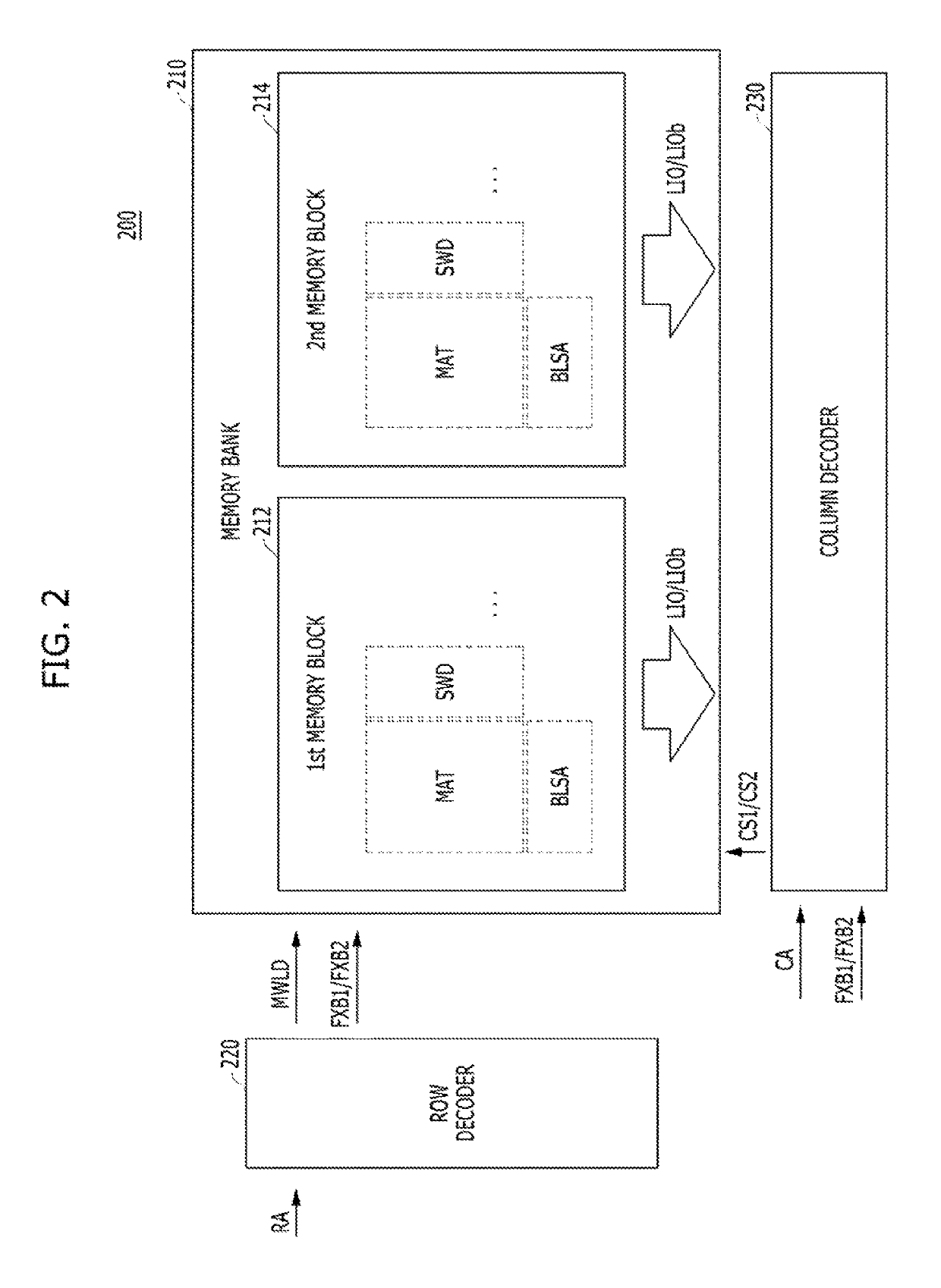
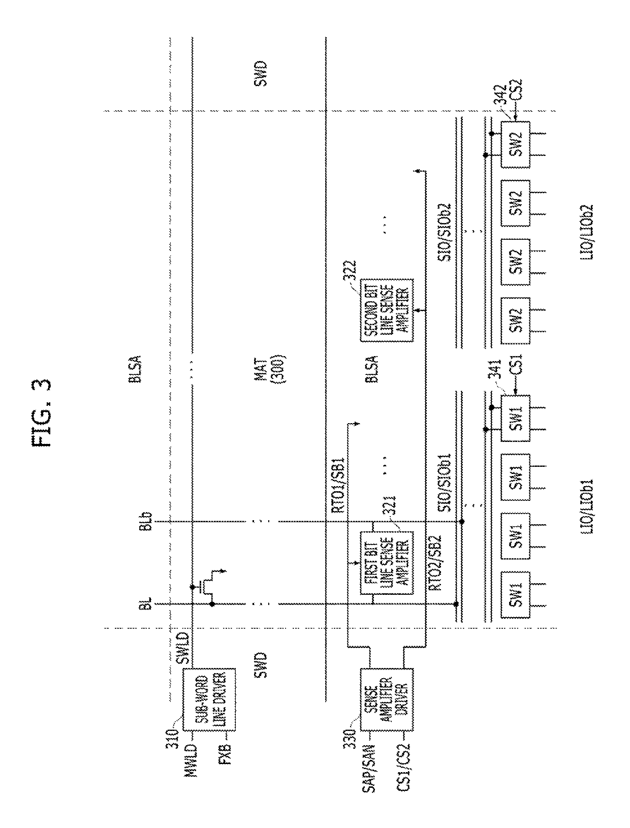
A memory device includes first and second memory blocks each including a memory cell array, a sub-word line drive region and a bit line sense amplifier region corresponding to the memory cell array, first and second data transmission lines disposed in the bit line sense amplifier region of each memory block, wherein the first and second data transmission lines extend on an identical row and transmit data of the memory cell array of the memory block, a row decoder configured to select one of the first and second memory blocks in response to a row address and enable a word line of the memory cell array included in the selected memory block, and a column decoder configured to generate, in response to a column address, first and second column select signals corresponding to the first and second data transmission lines of the bit line sense amplifier region.

Description

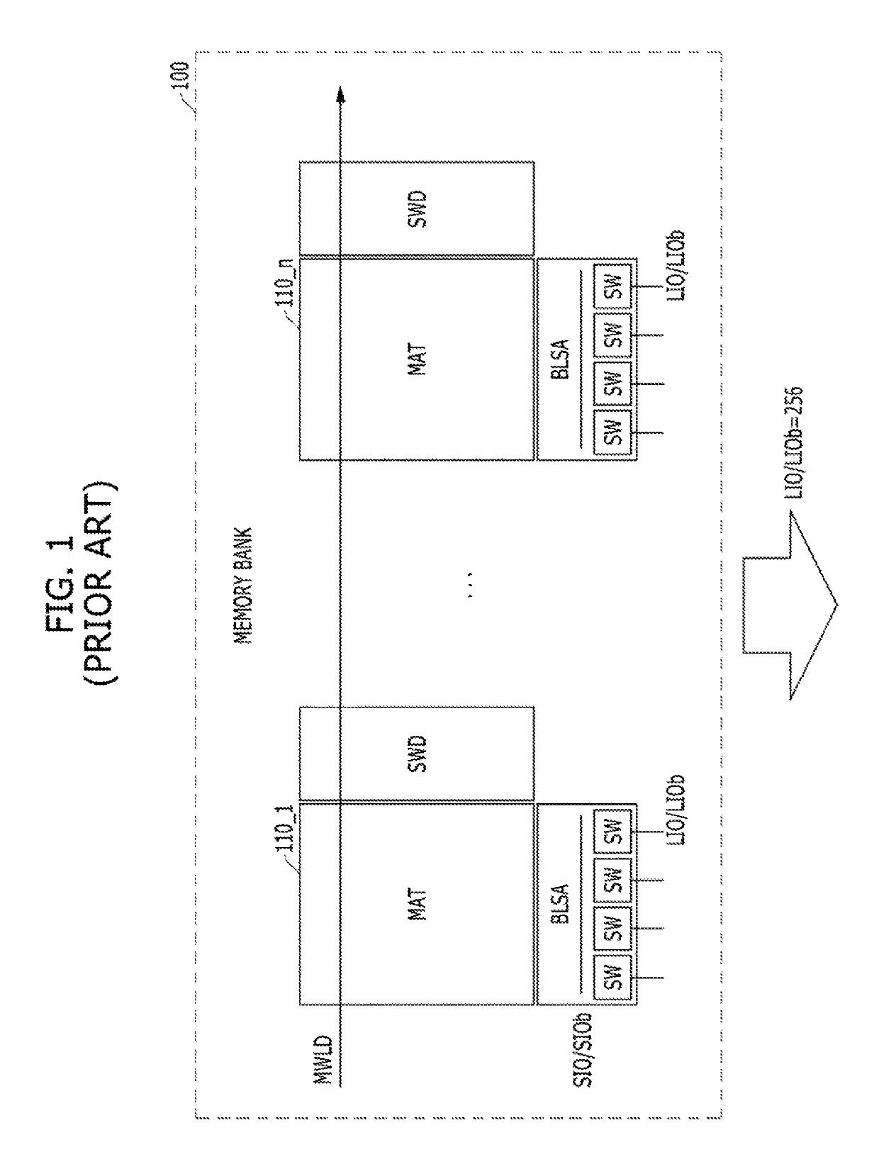
CROSS-REFERENCE TO RELATED APPLICATION[0001]This application claims priority under 35 U.S.C. § 119 to Korean Patent Application No. 10-2016-0167616 filed on Dec. 9, 2016 in the Korean Intellectual Property Office, the disclosure of which is incorporated herein by reference in its entirety.TECHNICAL FIELD[0002]Exemplary embodiments of the present disclosure relate to a semiconductor memory device, and more particularly, to a signal line layout structure for inputting / outputting data of a semiconductor memory device.DISCUSSION OF THE RELATED ART[0003]Generally, a semiconductor memory device may be divided into a core region including a memory bank, a row decoder, a column decoder, etc., and a peripheral region including a pad, a power supply circuit, a delay locked loop, etc.[0004]FIG. 1 is a block diagram illustrating a structure of a memory bank 100 of a conventional memory device.[0005]Referring to FIG. 1, the memory bank 100 is disposed in a core region of the memory device. The m...

Claims


Application Information

Patent Timeline
Patent Type & Authority Patents(United States)
IPC IPC(8): G11C7/10G11C5/02G11C7/08G11C5/06
CPCG11C7/1051G11C5/02G11C5/025G11C5/063G11C7/1069G11C7/1078G11C7/1048G11C2207/105G11C7/08G11C7/10G11C7/06G11C7/12G11C8/10G11C8/12
Inventor KIM, JONG-SUJUNG, YEON-GUL
Owner SK HYNIX INC
Learn More