Semiconductor integrated circuit device

a technology of integrated circuits and semiconductors, applied in semiconductor devices, semiconductor/solid-state device details, electrical apparatus, etc., can solve the problems of increasing the area of semiconductor integrated circuits, reducing the resistance value of common power supply interconnects, and increasing the interconnect resource requirements. , to achieve the effect of reducing the length of signal interconnects, reducing power consumption, and ensuring the effect of power supply ability

Active Publication Date: 2019-10-15
SOCIONEXT INC
View PDF12 Cites 0 Cited by
  • Summary
  • Abstract
  • Description
  • Claims
  • Application Information

AI Technical Summary

Benefits of technology

[0005]In the configuration disclosed in Japanese Unexamined Patent Publication No. 2000-21987, in which the I / O cells are arranged in multiple concentric rows, each I / O cell row is provided with a ring-shaped power supply interconnect, to which power is supplied through an external connection pad. This configuration requires each I / O cell row to have sufficient power supply ability and electrostatic discharge (ESD) protection capability. This requirement may be met by increasing the number of the I / O cells for power supply in each I / O cell row. Unfortunately, this solution further increases the area of the semiconductor integrated circuit.
[0006]It is therefore an object of the present disclosure to provide a configuration for a semiconductor integrated circuit device which is capable of ensuring sufficient power supply ability and ESD protection capability for an I / O cell, without causing an increase in the area of the semiconductor integrated circuit.
[0008]The semiconductor integrated circuit device according to this aspect includes at least two I / O cell rows, and a common power supply interconnect connects together a plurality of first I / O cells for supplying a power supply potential or a ground potential that are each included in a respective one of the I / O cell rows. The first I / O cells connected together via the common power supply interconnect are arranged so as to overlap with each other in the first direction. The common power supply interconnect extends in a second direction perpendicular to the first direction, and is connected to a first pad which is located closest to the common power supply interconnect in the first direction. This configuration enables each of the at least two I / O cell rows to be supplied with power from another one of the cell rows and to utilize the ESD protection function of another cell row. Thus, this configuration may enhance the power supply ability and the ESD protection capability without increasing the number of the I / O cells in each of the I / O cell rows. Further, this configuration may reduce an increase in interconnect resource required for the common power supply interconnect and keep an interconnect resistance value of the common power supply interconnect low.
[0010]According to this aspect, an internal logic circuit is arranged between the first and second I / O cell rows. The first I / O cell row is arranged inwardly from the internal logic circuit whereas the second I / O cell row is arranged outwardly from the internal logic circuit. The I / O cells in the first and second I / O cell rows are each divided into a high power supply voltage region and a low supply voltage region in a second direction that is perpendicular to the first direction, and are arranged such that each low power supply voltage region is located closer to the internal logic circuit. This configuration allows a reduction in the length of the signal interconnect that connects the internal logic circuit to the first I / O cell row located inwardly from the logic circuit in the semiconductor integrated circuit device. As a result, signals may be transmitted faster, and power consumption may be reduced.
[0011]The semiconductor integrated circuit device according to the present closure may ensure sufficient power supply ability and ESD protection capability for I / O cell rows, without increasing the area of the semiconductor integrated circuit.

Problems solved by technology

Unfortunately, this solution further increases the area of the semiconductor integrated circuit.
Further, this configuration may reduce an increase in interconnect resource required for the common power supply interconnect and keep an interconnect resistance value of the common power supply interconnect low.

Method used


Image

  • Semiconductor integrated circuit device
  • Semiconductor integrated circuit device
  • Semiconductor integrated circuit device

Examples


first embodiment

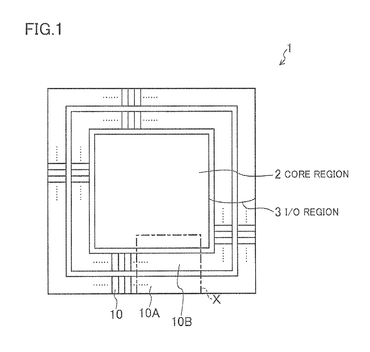
[0016]FIG. 1 is a plan view schematically illustrating an entire configuration for a semiconductor integrated circuit device according to an embodiment. The semiconductor integrated circuit device 1 illustrated in FIG. 1 includes a core region 2 in which an internal core circuit is provided, and an I / O region 3 which surrounds the core region 2 and in which an interface circuit (i.e., an I / O circuit) is provided. In the I / O region 3, two I / O cell rows 10A and 10B having a ring or frame shape extends along the periphery of the semiconductor integrated circuit device 1. Although not illustrated in detail in FIG. 1, a plurality of I / O cells 10 that form an interface circuit are arranged in each of the I / O cell rows 10A and 10B. Further, the semiconductor integrated circuit device 1 includes a plurality of external connection pads (not shown in FIG. 1) arranged therein.

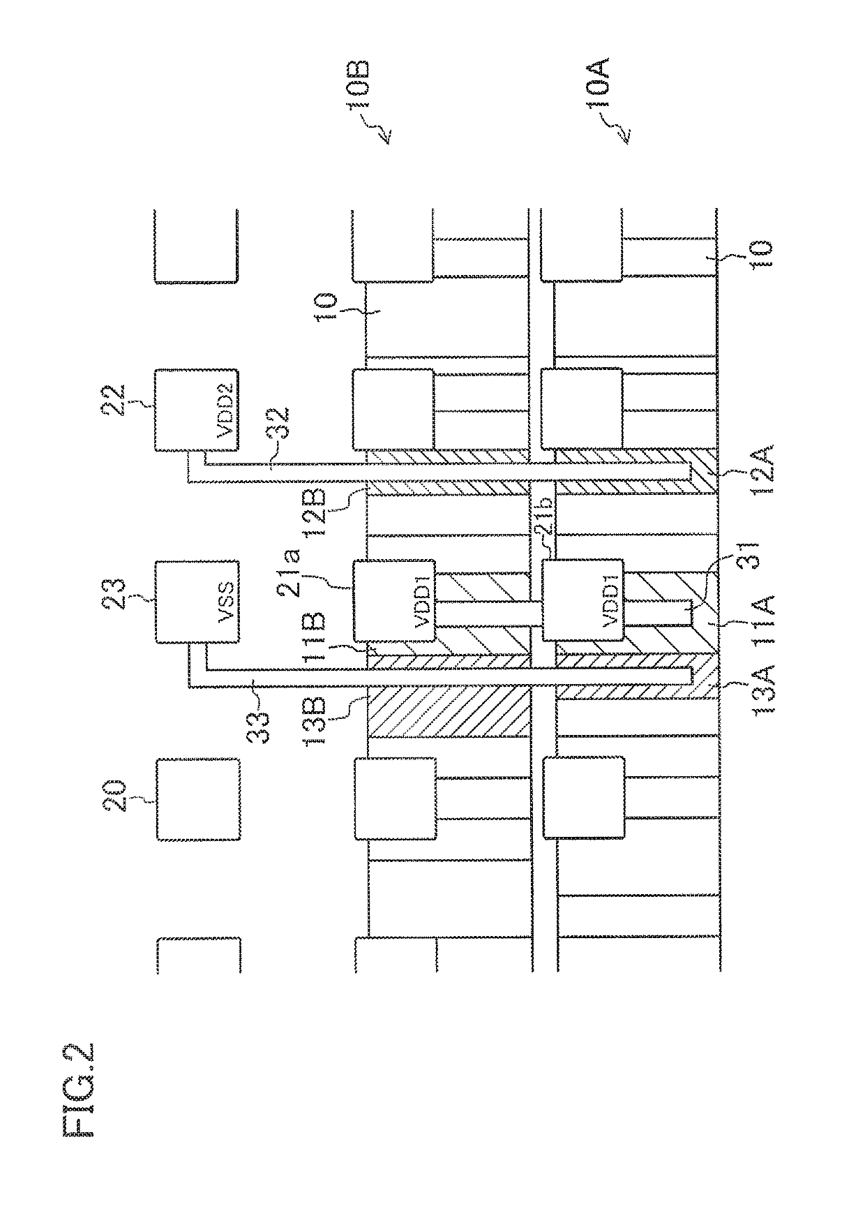
[0017]FIG. 2 illustrates an exemplary configuration for the I / O region 3 of the semiconductor integrated circuit device...

second embodiment

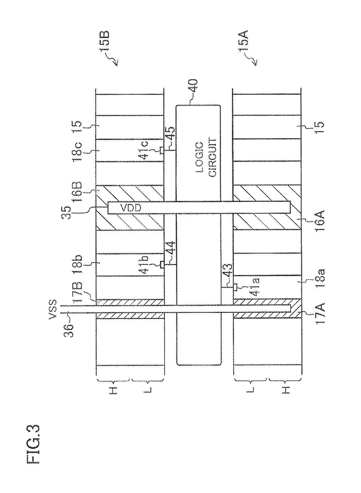
[0028]FIG. 3 illustrates an exemplary configuration for an I / O region 3 of a semiconductor integrated circuit device according to a second embodiment, and corresponds to an enlarged view of the portion X in FIG. 1. Note that FIG. 3 does not show an internal configuration for each I / O cell, signal interconnects, or other elements which do not constitute points of this embodiment. The configuration illustrated in FIG. 3 includes two I / O cell rows 15A and 15B, instead of the two I / O cell rows of 10A and 10B illustrated in FIG. 1. The I / O cell rows 15A and 15B each include a plurality of I / O cells 15 arranged in a horizontal direction in the figure which corresponds to a first direction. An internal logic circuit 40 is arranged between the I / O cell rows 15A and 15B. This internal logic circuit 40 between the I / O cell rows 15A and 15B forms part of an internal logic circuit which would be provided entirely in a core region 2 according to the known art. In the semiconductor integrated cir...


PUM


Abstract

Disclosed herein is a configuration for ensuring sufficient power supply ability and ESD protection capability for I / O cells in a semiconductor integrated circuit device, without increasing its circuit area. In two I / O cell rows, a pair of I / O cells for supplying a power supply potential or ground potential are connected together via a common power supply interconnect. The I / O cells are arranged so as to overlap with each other in a first direction in which the I / O cells are arranged. The common power supply interconnect extends in a second direction perpendicular to the first direction, and is connected to first pads that are located closest in the first direction to the common power supply interconnect.

Description

CROSS-REFERENCE TO RELATED APPLICATION[0001]This is a continuation of U.S. patent application Ser. No. 15 / 493,338 filed on Apr. 21, 2017, which is a continuation of International Application No. PCT / JP2015 / 004938 filed on Sep. 29, 2015, which claims priority to Japanese Patent Application No. 2014-217334 filed on Oct. 24, 2014. The entire disclosures of these applications are incorporated by reference herein.BACKGROUND[0002]The present disclosure relates to a semiconductor integrated circuit device including a core region and an I / O region.[0003]In recent years, semiconductor integrated circuits have further increased their scale to have an increasing number of input and output signals. Therefore, arranging input / output cells (I / O cells) in a single row to surround a core region may define the area of the semiconductor integrated circuit, thus increasing the area of a device including the semiconductor integrated circuit, i.e., a semiconductor integrated circuit device, which is not...

Claims


Application Information

Patent Timeline
Patent Type & Authority Patents(United States)
IPC IPC(8): H01L23/52H01L23/60H01L23/528H01L27/02H02H9/04
CPCH01L23/5286H01L27/0207H01L23/60H02H9/046
Inventor MATSUI, TOORUYOSHIMURA, MASAHIRO
Owner SOCIONEXT INC
Why Eureka
Try Eureka