Level shift circuit

a level shift circuit and level shift technology, applied in logic circuits, pulse automatic control, pulse techniques, etc., can solve problems such as difficult operation of level shift circuits, and achieve the effect of reliably operating level shift, reducing threshold voltage of n-type transistors, and reducing unit gate width of n-type transistors

Active Publication Date: 2009-03-12
SOCIONEXT INC
View PDF3 Cites 0 Cited by
  • Summary
  • Abstract
  • Description
  • Claims
  • Application Information

AI Technical Summary

Benefits of technology

[0028]According to the present invention, the plurality of gates are arranged at the rectangular doped region to align in the gate length direction with the gate width direction according with the short side direction of the doped region. As another option, the plurality of gates are arranged at each of the rectangular divided doped regions to align in the gate length direction with the gate width direction according with the short side direction of the doped region. With application of such layout, the unit gate width size of the n-type transistors can be reduced and thus, utilizing the above-described reverse narrow property, the threshold voltage of the n-type transistors can be reduced.
[0029]Thus, by using, as the pair of n-type transistors which receive an input signal and a reverse signal of the input signal as

Problems solved by technology

As a result, it becomes difficult

Method used


Image

  • Level shift circuit
  • Level shift circuit
  • Level shift circuit

Examples


first embodiment

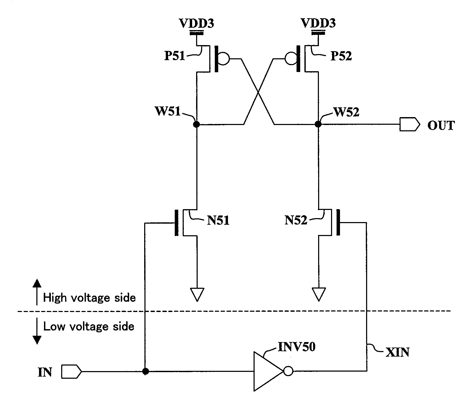
[0040]FIG. 1 is an exemplary configuration of a level shift circuit to which the present invention can be applied. The level shift circuit of FIG. 1 receives an input signal IN and outputs an output signal OUT obtained by converting a logic level of the input signal IN. A low voltage side circuit unit is operated by a first power supply voltage VDD and outputs the input signal IN and a reverse signal XIN of the input signal IN obtained by an inverter INV50 as a pair of complementary signals. A high voltage side circuit unit is operated by a second voltage VDD3 which is higher than the first power supply voltage VDD and includes n-type transistors N51 and N52 which receive the pair of complementary signals IN and XIN output from the low voltage side circuit unit at their gates, respectively. The detail operation of the level shift circuit is as described in the background of the invention and, therefore, the description thereof is omitted.

[0041]Note that the present invention is not ...

second embodiment

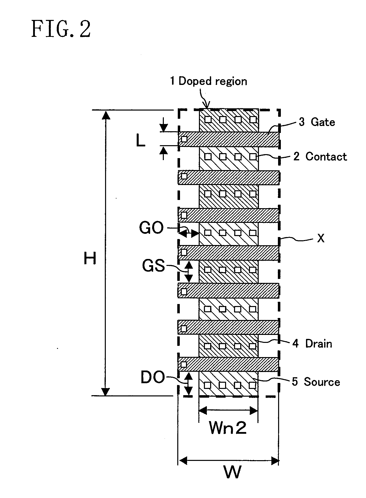
[0056]FIG. 4 is a view illustrating a specific layout configuration for a pair of n-type transistors in a level shift circuit, which receive a pair of complementary signals at their gates, respectively, according to this embodiment.

[0057]As shown in FIG. 4, each n-type transistor according to this embodiment includes a plurality (2 in FIG. 4) of divided rectangular doped regions 1A and 1B which function as drains 4 and sources 5, and a plurality of gates 3 arranged to align in a gate length direction with a gate width direction according with a short side direction of the doped regions 1A and 1B. Contacts 2 for making connection with wires are formed in each of the drains 4 and the sources 5. The drains 4 are connected with one another via wires. The gates 3 are connected with one another via wires. The sources 5 are connected with one another via wires. A unit gate width size is indicated by Wn2.

[0058]In the layout of FIG. 4, assuming that the number of gates is m and the number of...


PUM


Abstract

In a level shift circuit, even when a power supply voltage of an input signal is reduced, a level shift operation is reliably performed without causing increase in circuit area and process costs. For a pair of n-type transistors which receive an input signal and a reverse signal of the input signal as a pair of complementary signals at their gates, respectively, a layout which allows reduction in unit gate width size is adopted. The layout configuration includes a plurality of divided rectangular doped regions which function as drains and sources and a plurality of gates arranged to align in a gate length direction with a gate width direction according with a short side direction of the doped regions. The gates are electrically connected with one another, the drains are electrically connected with one another, and the sources are electrically connected with one another.

Description

CROSS-REFERENCE TO RELATED APPLICATION[0001]This application claims priority under 35 U.S.C. § 119(a) on Japanese Patent Application No. 2007-233654 filed on Sep. 10, 2007, the entire contents of which are hereby incorporated by reference.BACKGROUND OF THE INVENTION[0002]1. Field of the Invention[0003]The present invention relates to a level shift circuit for converting a logic level, and more particularly relates to a circuit configuration for performing a low voltage operation with low power consumption.[0004]2. Description of the Prior Art[0005]As a known level shift circuit, for example, a latch type level shift circuit has been known. A level shift circuit of this type is shown in FIG. 1.[0006]The level shift circuit of FIG. 1 includes two n-type transistors N51 and N52, cross-coupled two p-type transistors P51 and P52, and an inverter INV50. A gate of each of the p-type transistors P51 and P52 is connected to a drain of the other one of the p-type transistors P51 and P52. The ...

Claims


Application Information

Patent Timeline
IPC IPC(8): H03L5/00
CPCH03K3/35613H03K3/012
Inventor USAMI, SHIRO
Owner SOCIONEXT INC
Why Eureka
Try Eureka