Configuration of gate to drain (GD) clamp and ESD protection circuit for power device breakdown protection

a protection circuit and gate to drain technology, applied in semiconductor devices, diodes, semiconductor/solid-state device details, etc., can solve the problems of increasing the production cost of power devices, increasing the size of power devices, and limiting the conventional layout of manufacturing semiconductor power devices with protection circuits against breakdown and also against electrostatic discharge (esd). the effect of reducing the width of the gate to drain zener diodes

Active Publication Date: 2016-01-28
ALPHA & OMEGA SEMICON INC
View PDF2 Cites 12 Cited by
  • Summary
  • Abstract
  • Description
  • Claims
  • Application Information

AI Technical Summary

Benefits of technology

[0010]It is therefore an aspect of the present invention to provide a new and improved layout of an ESD protection circuit combined with gate-drain clamping on a semiconductor power device by forming a combination of gate to drain Zener diodes, a silicon diode and a small gate resistor for power MOSFETs' breakdown protection. The gate to drain Zener diode is only located at the one side of the die. Therefore, die size is reduced as compared to conventional design. Since the width of the gate to drain Zener diode is reduced, Idss leakage is low. No additional masks are needed as compared to a conventional power MOSFETs with polysilicon ESD diodes process. Gate to source Zener diodes may be added for ESD protection without any additional cost. It is another aspect of this invention that it provides a method to achieve a low Idss leakage, low resistance in gate to drain clamp with a smaller die size, therefore, low cost. It is another aspect of this invention to achieve a well-controlled breakdown voltage for the GD clamp, which is scalable to low voltage applications.

Problems solved by technology

Conventional layout for manufacturing semiconductor power devices with protection circuits against breakdown and also against electrostatic discharges (ESD) still has a limitation.
The configuration causes the die size to increase and therefore increases the production costs of the power devices.
Another technical difficulty is related to the great width of the gate to drain Zener diode.
The great width of the Zener diodes thus makes it difficult to limit the Idss leakage current under 10 μA that is generally required in many of such power device applications.
Furthermore, as discussed above, the Zener diodes formed around all the peripheral edges have a very large width thus causing the drain-source leakage Idss current to increase significantly and adversely affect the performance rating of the clamping circuits.
However, such device has a drawback that the polysilicon diodes occupy too much space wherein each stripe has a width of approximately five microns for protecting a breakdown voltage up to six volts.
With polysilicon diodes combined with Schottky diode or silicon diodes in these disclosures however the devices are limited to high breakdown voltage applications.
Furthermore, the breakdown voltage for these types of clamping devices is difficult to control.
Therefore, the GD clamping functions for device with low, well-controlled breakdown voltage applications with silicon diodes to supplement the back-to-back polysilicon diodes with space efficient configurations are still not available.
Another problem with the prior art methods of GD clamping is that the breakdown voltage at the ends of the silicon diodes have lower breakdown voltage (BV) than the rest of the silicon diode regions.
This will adversely affect the performance of the GD clamping by allowing current flow before the desired BV.
A conventional GD clamp comprising polysilicon diodes supplemented with a silicon or Schottky diode as disclosed in the prior art has difficulties in controlling the breakdown voltage.

Method used


Image

  • Configuration of gate to drain (GD) clamp and ESD protection circuit for power device breakdown protection
  • Configuration of gate to drain (GD) clamp and ESD protection circuit for power device breakdown protection
  • Configuration of gate to drain (GD) clamp and ESD protection circuit for power device breakdown protection

Examples


Embodiment Construction

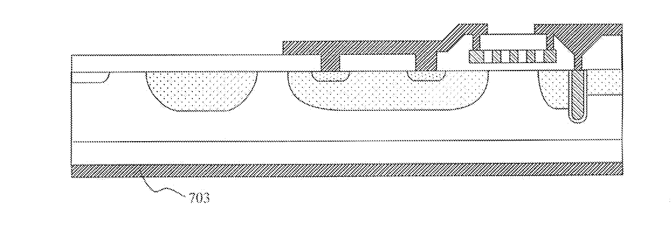
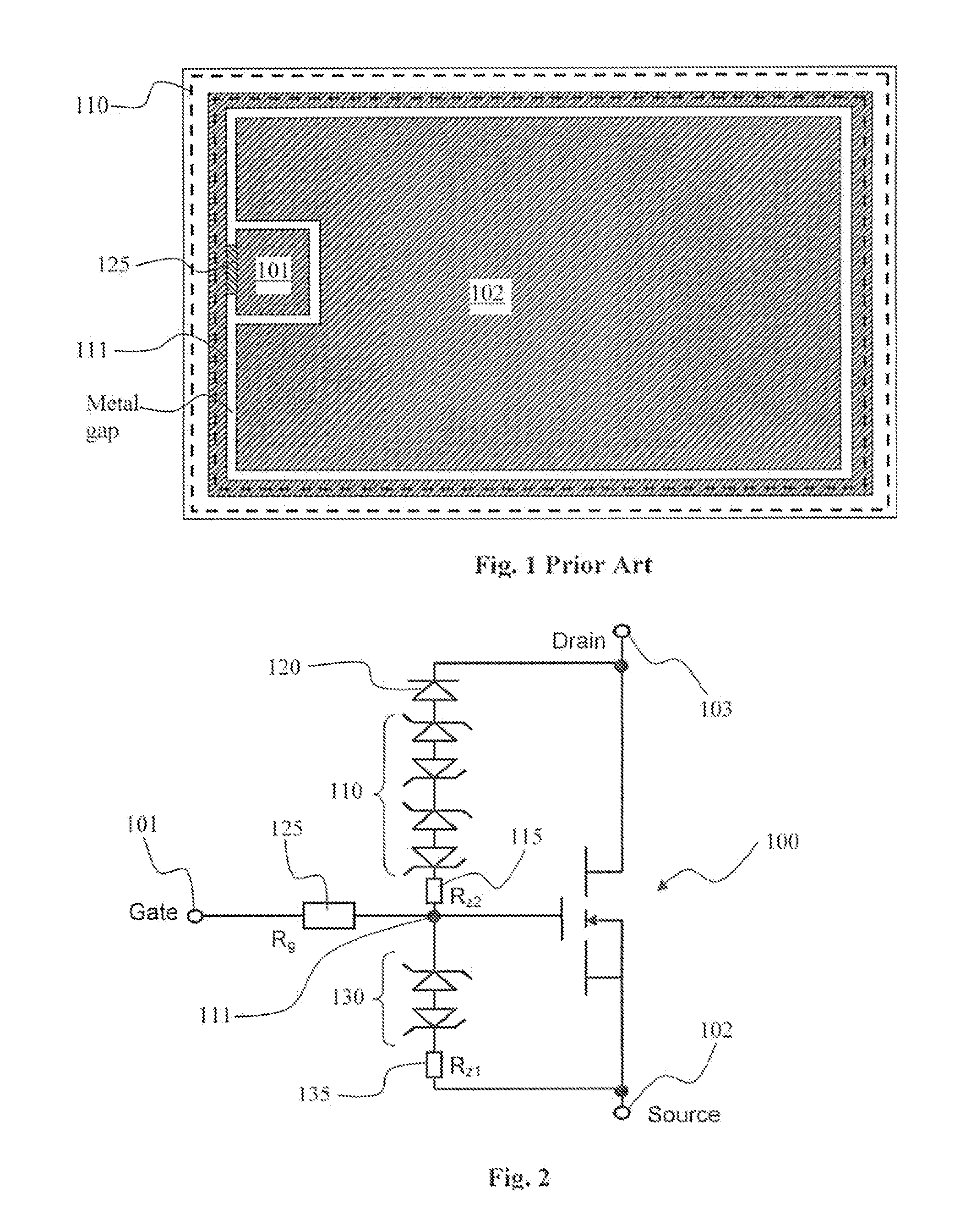
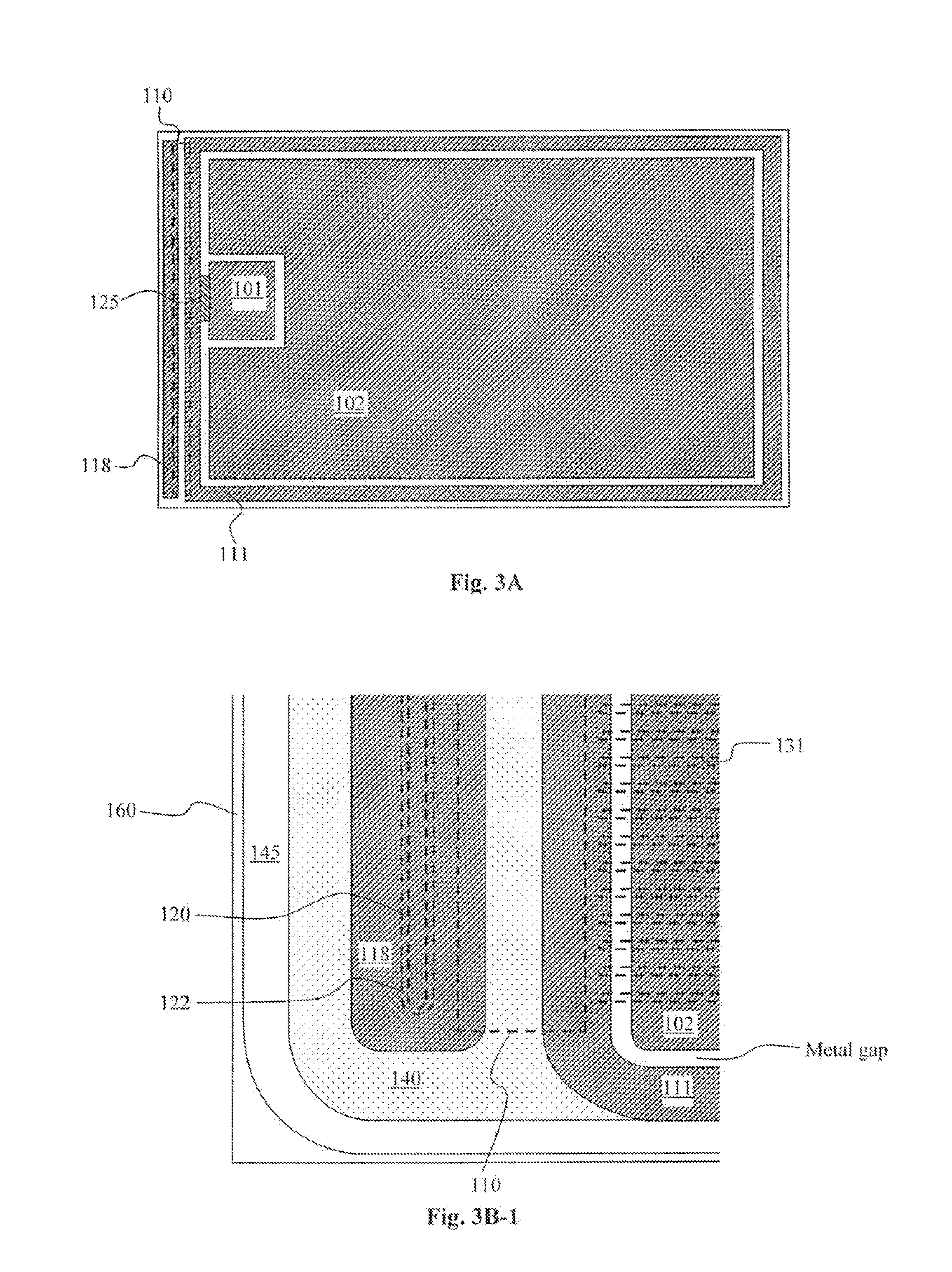
[0023]FIG. 2 is a circuit diagram to illustrate the breakdown protection circuit of a MOSFET device 100 of this invention. The MOSFET device has a gate electrode 101, a source electrode 102 and drain electrode 103. The GD clamp circuit applies a combination of gate to drain Zener diode pairs, shown as polysilicon diodes 110 with a parasitic resistance Rz2115, a silicon diode 120 and a small gate resistor Rg 125 to serve the function of breakdown protection for the power MOSFET. The Zener diode pairs 110 comprise back-to-back Zener diodes. In addition to the GD clamp circuit, the breakdown protection circuit may further comprise a gate-to-source ESD protection circuit including gate-to-source Zener diode pairs 130 with parasitic resistance Rz1115. FIGS. 3A-D below further illustrate that the gate to drain Zener diode pairs 110 that are formed at only one side of the die. Therefore, die size is reduced as compared to conventional design. The GD clamp circuit is electrically connected ...


PUM


Abstract

A semiconductor power device supported on a semiconductor substrate comprising a plurality of transistor cells each having a source and a drain with a gate to control an electric current transmitted between the source and the drain. The semiconductor further includes a gate-to-drain (GD) clamp termination connected in series between the gate and the drain further includes a plurality of back-to-back polysilicon diodes connected in series to a silicon diode includes parallel doped columns in the semiconductor substrate wherein the parallel doped columns having a predefined gap. The doped columns further include a U-shaped bend column connect together the ends of parallel doped columns with a deep doped-well that is disposed below and engulfing the U-shaped bend.

Description

[0001]This Patent Application is a Continuation Application and claims the Priority Date of a co-pending application Ser. No. 12 / 932,584 filed on Feb. 28, 2011 by common Inventors of this Application. application Ser. No. 12 / 932,584 is a Divisional Application of another Patent application Ser. No. 12 / 378,039 filed on Feb. 9, 2009 now issued into U.S. Pat. No. 8,441,109. The Disclosures made in the patent application Ser. No. 12 / 932,584 and Ser. No. 12 / 378,039 are hereby incorporated by reference.BACKGROUND OF THE INVENTION[0002]1. Field of the Invention[0003]The invention relates generally to the layout and manufacturing process of the semiconductor power devices. More particularly, this invention relates to an improved configuration of gate-to-drain (GD) clamp combined with the electrostatic discharge (ESD) protection circuit for power device breakdown protection to achieve smaller die size, reduced leakage currents, better control of the GD clamp breakdown voltage and lower produ...

Claims


Application Information

Patent Timeline
Patent Type & Authority Applications(United States)
IPC IPC(8): H01L27/02H01L27/06
CPCH01L27/0629H01L27/0255
Inventor SU, YIBHALLA, ANUPNG, DANIEL
Owner ALPHA & OMEGA SEMICON INC
Why Eureka
Try Eureka