Shielded gate mosfet-schottky rectifier-diode integrated circuits with trenched contact structures

a technology of integrated circuits and contact structures, which is applied in the direction of diodes, semiconductor devices, electrical apparatus, etc., can solve the problems of poor performance and high manufacturing cost, and achieve the effects of improving the configuration of semiconductor power devices, reducing die size and cos

Active Publication Date: 2013-01-24
FORCE MOS TECH CO LTD
View PDF1 Cites 14 Cited by
  • Summary
  • Abstract
  • Description
  • Claims
  • Application Information

AI Technical Summary

Benefits of technology

[0005]It is therefore another aspect of the present invention to provide improved semiconductor power device configuration for providing an integrated circuit comprising trench MOSFET with embedded Schottky rectifier and Gate-Source clamp diode on single chip to achieve reduced die size, lower cost and improved performance. According to the present invention, the integrated circuit comprising: a substrate of a first conductivity type; an epitaxial layer of the first conductivity type over the substrate, the epitaxial layer having a lower doping concentration than the substrate; a trench MOSFET comprising a plurality of shielded trenched gates in the epitaxial layer, wherein each the shielded trenched gate comprising a gate electrode disposed in the upper portion and a shielded electrode disposed in the lower portion of a first type gate trench, wherein the gate electrode and the shielded electrode insulated from each other by an inter-electrode insulation layer; each the shielded trenched gate comprising a first type gate oxide surrounding bottom and sidewalls of the shielded electrode and a second type gate oxide along sidewalls of the gate electrode, wherein the first type gate oxide having thickness greater than the second type gate oxide; the gate electrode in the first gate trench being surrounded by a source region of the first conductivity type encompassed in a body region of a second conductivity type, the gate electrode being connected to a gate metal; the shielded electrode in the first type gate trench being surrounded by the epitaxial layer and being connected to a source metal; a Schottky rectifier extending into the epitaxial layer and having a Schottky barrier layer lined in a trenched anode contact filled with a contact metal plug; and a Gate-Source clamp diode comprising multiple back to back poly-silicon Zener diodes with alternating doped regions of the first conductivity type next to the second conductivity type, connected with the gate metal on one side, and with the source metal on another side.
[0006]It is therefore another aspect of the present invention to provide improved semiconductor power device configuration for providing an integrated circuit comprising trench MOSFET with embedded Schottky rectifier, and Gate-Drain clamp diode on single chip to achieve reduced die size, lower cost and improved performance. According to the present invention, the integrated circuit comprising: a substrate of a first conductivity type; an epitaxial layer of the first conductivity type over the substrate, the epitaxial layer having a lower doping concentration than the substrate; a trench MOSFET comprising a plurality of shielded trenched gates in the epitaxial layer, wherein each the shielded trenched gate comprising a gate electrode disposed in the upper portion and a shielded electrode disposed in the lower portion of a first type gate trench, wherein the gate electrode and the shielded electrode insulated from each other by an inter-electrode insulation layer; each the shielded trenched gate comprising a first type gate oxide surrounding bottom and sidewalls of the shielded electrode and a second type gate oxide along sidewalls of the gate electrode, wherein the first type gate oxide having thickness greater than the second type gate oxide; the gate electrode in the first gate trench being surrounded by a source region of the first conductivity type encompassed in a body region of a second conductivity type, the gate electrode being connected to a gate metal; the shielded electrode in the first type gate trench being surrounded by the epitaxial layer and being connected to a source metal; a Schottky rectifier extending into the epitaxial layer and having a Schottky barrier layer lined in a of trenched anode contact filled with a contact metal plug; and a Gate-Drain clamp diode comprising multiple back to back poly-silicon Zener diodes with alternating doped regions of the first conductivity type next to the second conductivity type, connected with the gate metal on one side and with a drain metal on another side through a plurality of metal stripes cross over a termination area.
[0007]It is therefore another aspect of the present invention to provide improved semiconductor power device configuration for providing an integrated circuit comprising trench MOSFET with Gate-Drain clamp diode and Gate-Source clamp diode on single chip to achieve reduced die size, lower cost and improved performance. According to the present invention, the integrated circuit comprising: a substrate of a first conductivity type; an epitaxial layer of the first conductivity type over the substrate, the epitaxial layer having a lower doping concentration than the substrate; a trench MOSFET comprising a plurality of shielded trenched gates in the epitaxial layer, wherein each the shielded trenched gate comprising a gate electrode disposed in the upper portion and a shielded electrode disposed in the lower portion of a first type gate trench, wherein the gate electrode and the shielded electrode insulated from each other by an inter-electrode insulation layer; each the shielded trenched gate comprising a first type gate oxide surrounding bottom and sidewalls of the shielded electrode and a second type gate oxide along sidewalls of the gate electrode, wherein the first type gate oxide having thickness greater than the second type gate oxide; the gate electrode in the first gate trench being surrounded by a source region of the first conductivity type encompassed in a body region of a second conductivity type, the gate electrode being connected to a gate metal; the shielded electrode in the first type gate trench being surrounded by the epitaxial layer and being connected to a source metal; a Gate-Drain clamp diode comprising multiple back to back poly-silicon Zener diodes with alternating doped regions of the first conductivity type next to the second conductivity type, connected with the gate metal on one side and with a drain metal on another side through a plurality of metal stripes cross over a termination area; and a Gate-Source clamp diode comprising multiple back to back poly-silicon Zener diodes with alternating doped regions of the first conductivity type next to the second conductivity type, connected with the gate metal on one side, and with the source metal on another side.
[0008]It is therefore another aspect of the present invention to provide improved semiconductor power device configuration for providing an integrated circuit comprising trench MOSFET with Gate-Source clamp diode on single chip to achieve reduced die size, lower cost and improved performance. According to the present invention, the integrated circuit comprising: a substrate of a first conductivity type; an epitaxial layer of the first conductivity type over the substrate, the epitaxial layer having a lower doping concentration than the substrate; a trench MOSFET comprising a plurality of shielded trenched gates in the epitaxial layer, wherein each the shielded trenched gate comprising a gate electrode disposed in the upper portion and a shielded electrode disposed in the lower portion of a first type gate trench, wherein the gate electrode and the shielded electrode insulated from each other by an inter-electrode insulation layer; each the shielded trenched gate comprising a first type gate oxide surrounding bottom and sidewalls of the shielded electrode and a second type gate oxide along sidewalls of the gate electrode, wherein the first type gate oxide having thickness greater than the second type gate oxide; the gate electrode in the first gate trench being surrounded by a source region of the first conductivity type encompassed in a body region of a second conductivity type, the gate electrode being connected to a gate metal; the shielded electrode in the first type gate trench being surrounded by the epitaxial layer and being connected to a source metal; and a Gate-Source clamp diode comprising multiple back to back poly-silicon Zener diodes with alternating doped regions of the first conductivity type next to the second conductivity type, connected with the gate metal on one side, and with the source metal on another side.
[0009]It is therefore another aspect of the present invention to provide improved semiconductor power device configuration for providing an integrated circuit comprising trench MOSFET with Gate-Drain clamp diode on single chip to achieve reduced die size, lower cost and improved performance. According to the present invention, the integrated circuit comprising: a substrate of a first conductivity type; an epitaxial layer of the first conductivity type over the substrate, the epitaxial layer having a lower doping concentration than the substrate; a trench MOSFET comprising a plurality of shielded trenched gates in the epitaxial layer, wherein each the shielded trenched gate comprising a gate electrode disposed in the upper portion and a shielded electrode disposed in the lower portion of a first type gate trench, wherein the gate electrode and the shielded electrode insulated from each other by an inter-electrode insulation layer; each the shielded trenched gate comprising a first type gate oxide surrounding bottom and sidewalls of the shielded electrode and a second type gate oxide along sidewalls of the gate electrode, wherein the first type gate oxide having thickness greater than the second type gate oxide; the gate electrode in the first gate trench being surrounded by a source region of the first conductivity type encompassed in a body region of a second conductivity type, the gate electrode being connected to a gate metal; the shielded electrode in the first type gate trench being surrounded by the epitaxial layer and being connected to a source metal; a Gate-Drain clamp diode comprising multiple back to back poly-silicon Zener diodes with alternating doped regions of the first conductivity type next to the second conductivity type, connected with the gate metal on one side and with a drain metal on another side through a plurality of metal stripes cross over termination area.
[0010]In some other preferred embodiments, the present invention can be implemented including one or more following features: the trench MOSFET further comprising a second type gate trench being filled with a single shielded electrode having same conductive material as the shielded electrode in the shielded trenched gates in the trench MOSFET, padded by the first type gate oxide, wherein the single shielded electrode in the second type gate trench being connected to the source metal through a trenched shielded electrode contact filled with the contact metal plug; the Schottky rectifier is a trench Schottky rectifier having a Schottky barrier layer lined in the trenched anode contact filled with the contact metal plug, and disposed between a pair of adjacent third type gate trenches, each of the third type gate trenches filled with a single shielded electrode having same conductive material as the shielded electrode in the shielded trenched gates in the trench MOSFET, padded by the first type gate oxide; the Schottky rectifier is a trench Schottky rectifier having a Schottky barrier layer lined in the trenched anode contact filled with the contact metal plug, and disposed between a pair of adjacent third type gate trenches, each of the third type gate trenches filled with a gate electrode and a shielded electrode having same conductive material and structure as the shielded trenched gates in the trench MOSFET; the Schottky rectifier is a Junction Barrier Schottky (JBS) rectifier having a Schottky barrier layer lined in the trenched anode contact filled with the contact metal plug and between a pair of the adjacent body regions; the Schottky rectifier further comprising a Schottky barrier enhancement region of the first conductivity type surrounding sidewalls and bottom of each the trenched anode contact in the epitaxial layer, the Schottky barrier height enhancement region having doping concentration lower than the epitaxial layer; the Schottky rectifier further comprises a Schottky barrier height enhancement region of the second conductivity type surrounding sidewalls and bottom of each the trenched anode contact in the epitaxial layer; the Gate-Source clamp diode being connected to the source metal through a first trenched diode contact filled with the contact metal plug, and being connected to the gate metal through a second trenched diode contact filled with the contact metal plug; the Gate-Drain clamp diode being connected to the gate metal through a third trenched diode contact filled with the contact metal plug, and being connected to the drain metal through a forth trenched diode contact filled with the contact metal plug; the integrated circuit further comprises etch-buffer trenched gates disposed in the epitaxial layer underneath each of the first, second, third and forth trenched diode contacts to serve as buffer layers for prevention of gate-body shortage.

Problems solved by technology

However, assembly of those separate structures into single package with extra interconnection wires results in higher manufacturing cost, and poor performance due to increase in inductance from the extra interconnection wires.

Method used


Image

  • Shielded gate mosfet-schottky rectifier-diode integrated circuits with trenched contact structures
  • Shielded gate mosfet-schottky rectifier-diode integrated circuits with trenched contact structures
  • Shielded gate mosfet-schottky rectifier-diode integrated circuits with trenched contact structures

Examples


Embodiment Construction

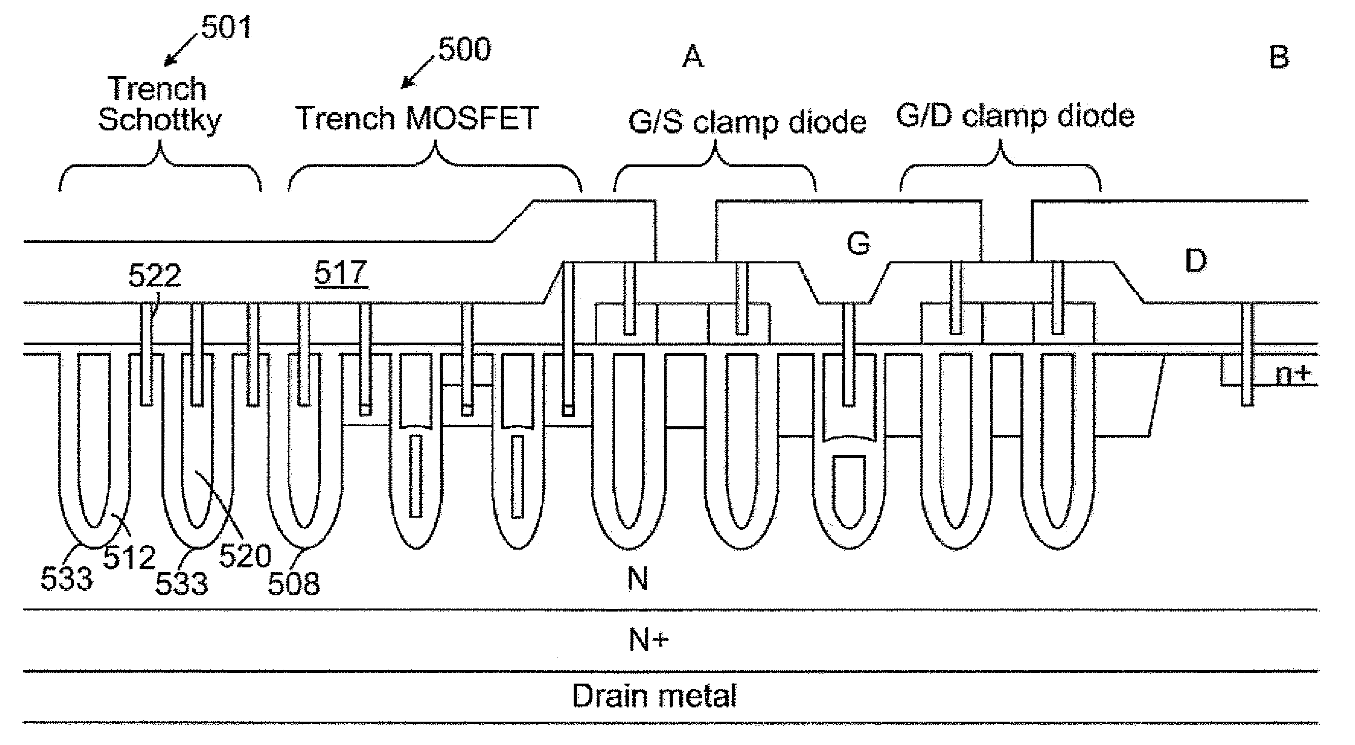
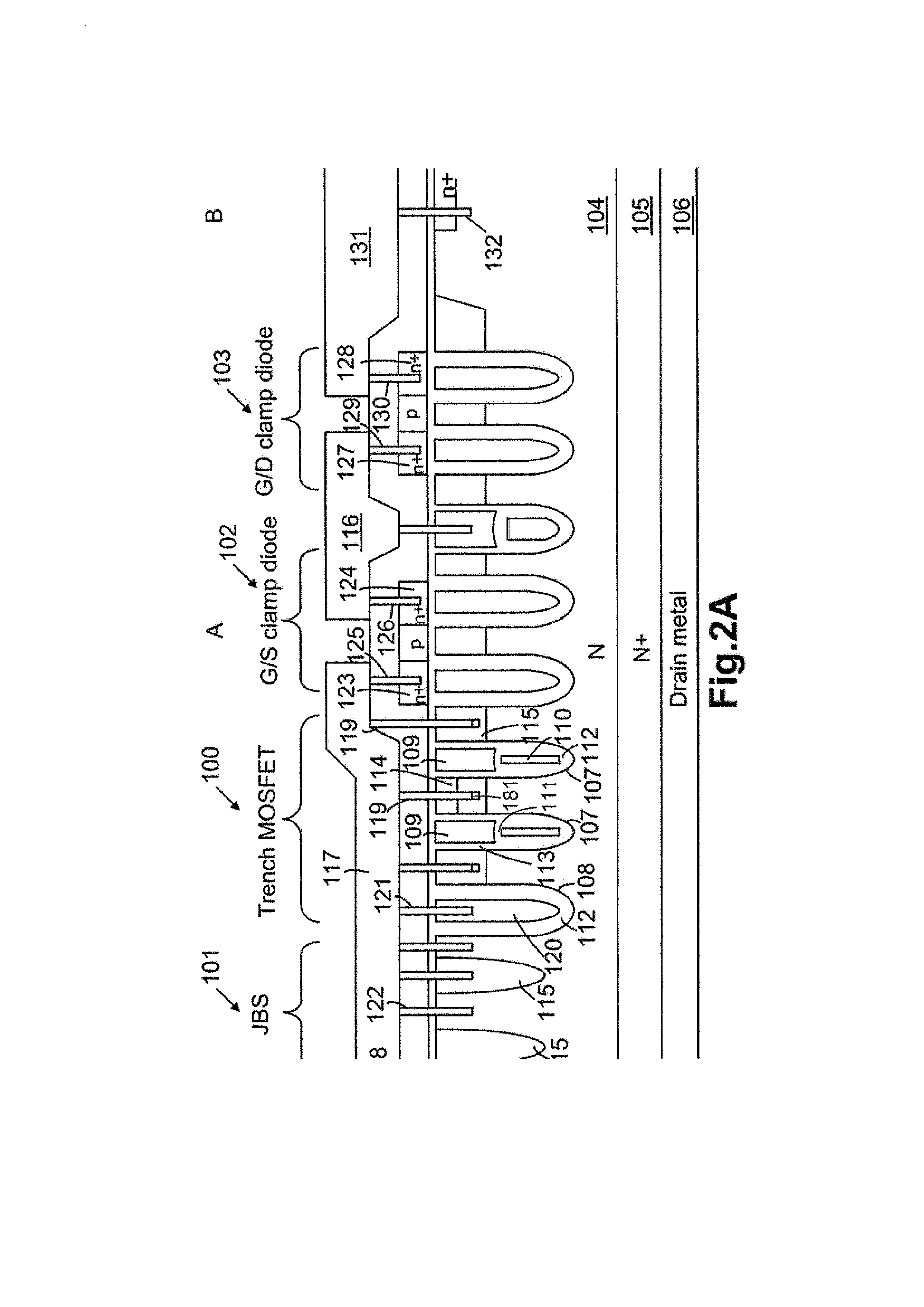
[0021]Please refer to FIG. 2A and FIG. 2B for a preferred embodiment of this invention which is respective A-B and C-D cross-sectional view of FIG. 2C. In FIG. 2A, an N-channel trench MOSFET 100 is implemented with Junction Barrier Schottky rectifier 101 (JBS, as illustrated), a Gate-Source clamp diode 102 (GIS clamp diode, as illustrated) and a Gate-Drain clamp diode 103 (G / D clamp diode, as illustrated) in an N epitaxial layer 104 above an N+ substrate 105 which is coated with back metal of Ti / Ni / Ag on rear side as drain metal 106. The trench MOSFET 100 further comprises a plurality of first type gate trenches 107 for shielded trenched gates and a second type gate trench 108 for shielded electrode contact, wherein each the first type gate trench 107 is filled with a gate electrode 109 in the upper portion and a shielded electrode 110 in the lower portion, wherein the gate electrode 109 is insulated from the shielded electrode 110 by an inter-electrode insulation layer 111. Besides...


PUM


Abstract

A trench shielded gate MOSFET device with embedded Schottky rectifier, Gate-Drain and Gate-Source clamp diodes on single chip is formed to achieve device shrinkage, lower cost and improved performance. The present semiconductor device achieve low Vf and reverse leakage current for embedded Schottky rectifier, having over-voltage protection and avalanche protection between gate and source and between gate and drain.

Description

FIELD OF THE INVENTION[0001]This invention relates generally to the cell structure, device configuration and fabricating method of power semiconductor devices. More particularly, this invention relates to an improved cell configuration to manufacture trench shielded gate MOSFET (Metal Oxide Semiconductor Field Effect Transistor) with Schottky rectifier diode, Gate-Drain (GD) and Gate-Source (GS) clamp diode on single chip for device shrinkage and performance improvement.BACKGROUND OF THE INVENTION[0002]Please refer to FIG. 1, normally for high efficiency DC / DC application, a Schottky rectifier is externally added in parallel with a MOSFET device to prevent a parasitic P / N body diode in the MOSFET from turning on in order to achieve higher speed and efficiency. The requirement for clamping effect is that the forward voltage of the Schottky rectifier Vf is less than the parasitic P / N body diode (˜0.7V). Besides, for providing effective ESD (electrostatic discharge) protection between ...

Claims


Application Information

Patent Timeline
Patent Type & Authority Applications(United States)
IPC IPC(8): H01L27/06
CPCH01L27/0629H01L29/8725H01L29/407H01L29/7806H01L29/7808H01L29/7811H01L29/7813H01L29/0619H01L29/0638H01L29/0653H01L29/0696H01L29/0878H01L29/861H01L29/872H01L29/402
Inventor HSIEH, FU-YUAN
Owner FORCE MOS TECH CO LTD
Why Eureka
Try Eureka