Mirror device

a mirror device and light modulator technology, applied in the field of mirror devices, can solve the problems of adverse effects on image quality, limited image display quality, and limited image quality, so as to prevent adverse effects and improve device configurations.

Active Publication Date: 2010-01-26
IGNITE INC +1
View PDF26 Cites 4 Cited by
  • Summary
  • Abstract
  • Description
  • Claims
  • Application Information

AI Technical Summary

Benefits of technology

[0045]In consideration of the technical difficulties and limitations encountered by the conventional mirror devices as described above, an aspect of the present invention is to manufacture a mirror device with new manufacturing processes with improved device configurations. The improved manufacturing processes and device configurations are implemented for preventing the adverse effects attributable to the incident light projected to a protective layer on a substrate. According to the present invention, a mirror device comprises: an electrode covered with a protective film composed of a semiconductor disposed on a substrate; a mirror disposed above the electrode; and an electrically conductive hinge placed between the mirror and the electrode, wherein an opening part is formed in a part of the protective film, and the hinge penetrates the protective film in the opening part thereof.

Problems solved by technology

Even though there are significant advances of the technologies for implementing an electromechanical mirror device as a spatial light modulator (SLM) in recent years, there are still limitations and difficulties when it is employed to display a high quality image.
Specifically, when the images are digitally controlled, the image quality is adversely affected due to the fact that the images are not displayed with sufficient number of gray scales.
The quality of an image display is limited due to the limited number of gray scales.
Specifically, in a conventional control circuit that applies a PWM (Pulse Width Modulation), the quality of the image is limited by the LSB (least significant bit) or the least pulse width as a control related to the ON or OFF state.
Since the mirror is controlled to operate in either the ON or OFF state, the conventional image display apparatus has no way to provide a pulse width for controlling the mirror that is shorter than the control duration allowable on the basis of the LSB.
The limited number of gray scales leads to a degradation of the image.
In this configuration, a reflected light spreading outside of an angular ranges specifically designed for image display may inadvertently generated from the gaps between adjacent mirrors.
The reflections generated from the gaps between the mirrors have an undesirable effect of degrading the contrast of an image display.
As a result, the quality of the image display is adversely affected.
That leads to the degradations of image qualities.
The artifacts are caused by a technical limitation that the digitally controlled image display is not controlled by a sufficient number of gray scales, i.e. the levels of the quantity of light.
Such problems are particularly caused by the fact that the mirrors are controlled either at the ON or OFF position.
The mirrors produced by applying the CMOS technologies probably is not appropriate for operating the mirror at such a high range of voltages, and therefore the DMOS mirror devices may be required.
Conventional mirror are therefore faced with a technical difficulty that in order to produce image display device with smaller size it may be necessary to sacrifice high quality of image display with a higher level of gray scales due to a higher range of the operable voltages.
However, these patents or patent applications do not provide an effective solution to attain a sufficient number of the gray scales in the digitally controlled image display system.
However, these inventions do not provide a direct solution for a person skilled in the art to overcome the above-discussed limitations and difficulties.
The heat propagated in the protective film covering over the hinge of the mirror device may also adversely affect the mirror operations due to the effects to the changes to the Coulomb force with the heat propagation changing the operational characteristics of the elastic hinges.
These patented and published disclosures related to the mirror device and hinge configurations and structures, however do not provide improved methods and device configurations to resolve the above discussed difficulties and limitations.

Method used


Image

  • Mirror device
  • Mirror device
  • Mirror device

Examples


Embodiment Construction

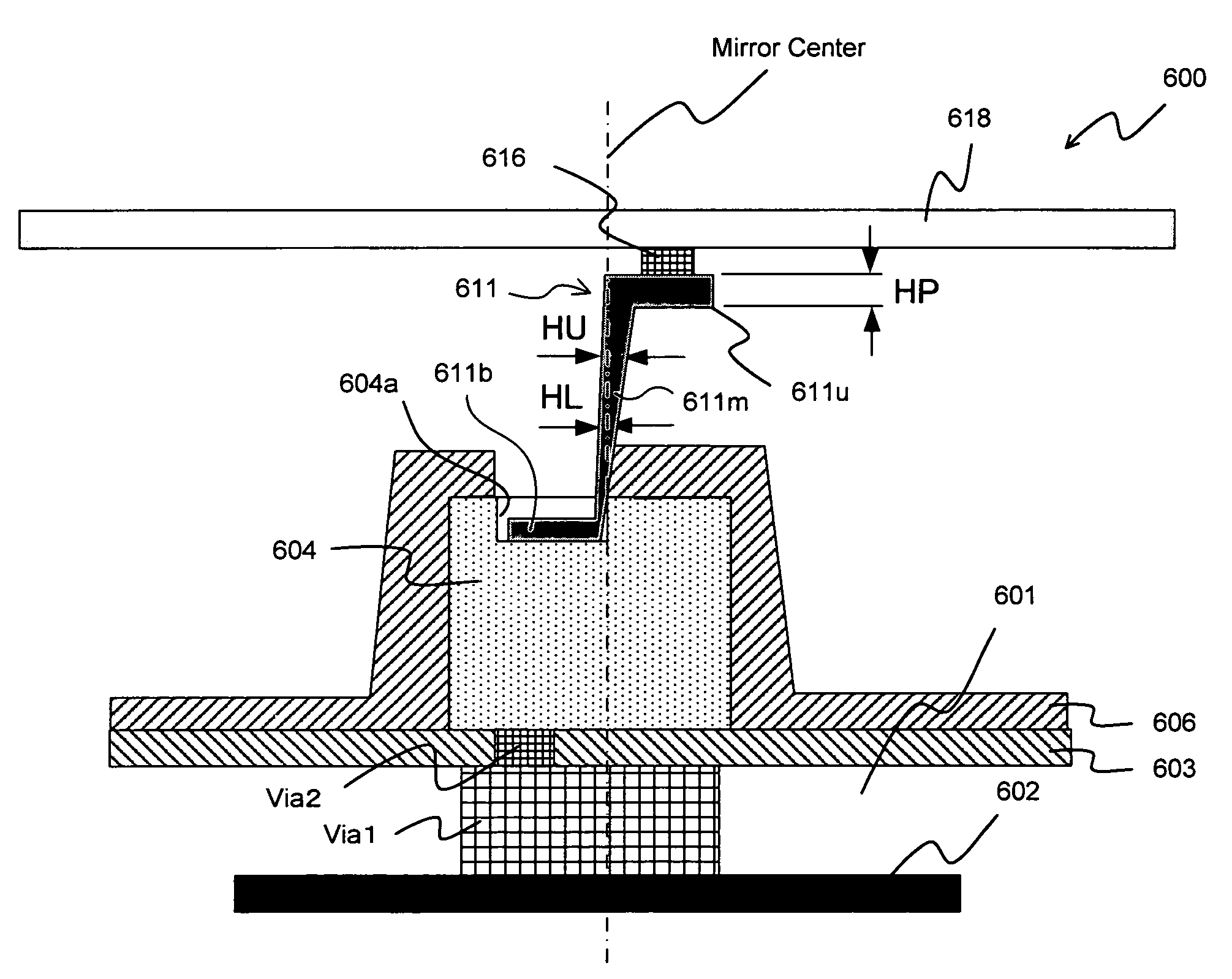
[0077]A mirror device implemented in a projection apparatus according to a preferred embodiment of the present invention is described below by referring to the accompanying drawings.

[0078]FIGS. 5A through 5F are cross-sectional diagrams for describing the processing steps for producing a mirror device according to a preferred embodiment of the present invention.

[0079]FIG. 5A shows the step 1 to form a wiring 502 of a drive circuit for driving and controlling a mirror (which is described later) in a semiconductor wafer substrate (simply noted as “substrate” hereinafter) 501. A cavity as an opening part (i.e., a cavity or concave part) 501a is opened from a top surface of the substrate 501 and extends to the upper surface of the wiring 502 preferably composed of aluminum. A first protective layer, i.e., a protective film, 503 is deposited on the parts of the substrate 501 except for the opening part 501a. The first protective layer 503 is deposited before the opening part 501a of the ...


PUM


Abstract

A mirror device comprises: an electrode which is covered with a protective film made of a material containing a semiconductor material and is placed on a substrate; a mirror placed above the electrode; and an electrically conductive hinge placed between the mirror and the electrode, wherein an opening part is formed in a part of the protective film, and the hinge penetrates the protective film in the opening part thereof.

Description

CROSS REFERENCE TO RELATED APPLICATIONS[0001]This application is Continuation in Part (CIP) Application of a Co-Pending patent application Ser. No. 11 / 894,248 filed on Aug. 18, 2007 by one of the common Inventors of this patent application. Application Ser. No. 11 / 894,248 is a Non-provisional application of a Provisional application 60 / 841,173 filed on Aug. 30, 2006. The Provisional Application 60 / 839,637 is a Continuation in Part (CIP) Application of a pending U.S. patent application Ser. Nos. 11 / 121,543 filed on May 4, 2005. The application Ser. No. 11 / 121,543 is a Continuation in part (CIP) Application of three previously filed Applications. These three Applications are U.S. application Ser. Nos. 10 / 698,620 filed on Nov. 1, 2003, 10 / 699,140 filed on Nov. 1, 2003, and 10 / 699,143 filed on Nov. 1, 2003 by one of the Applicants of this patent application. The disclosures made in these patent applications are hereby incorporated by reference in this patent application.BACKGROUND OF TH...

Claims


Application Information

Patent Timeline
Patent Type & Authority Patents(United States)
IPC IPC(8): G02B26/00G02B26/08
CPCG02B26/0841
Inventor ISHII, FUSAOMAEDA, YOSHIHIROICHIKAWA, HIROTOSHISUGIMOTO, NAOYA
Owner IGNITE INC
Why Eureka
Try Eureka