Formation method of gate electrode in a semiconductor process

Inactive Publication Date: 2006-04-18
DONGBU ELECTRONICS CO LTD
View PDF23 Cites 3 Cited by
  • Summary
  • Abstract
  • Description
  • Claims
  • Application Information

AI Technical Summary

Benefits of technology

[0014]In consideration of the above problem, it is an object of the present invention to provide a method of forming a gate electrode in a semiconductor device, which is capable of reducing a line width of the gate electrode by performing a photolithography process after defining a wide region on which a gate electrode is located on a photoresist twice such that the line width of the gate electrode is not subject to a wavelength of a light source used when the photolithography process is performed.

Problems solved by technology

However, since the line width of the gate electrode, which is the most narrow line width of all line widths of elements in the semiconductor device, is destined to be limited by the wavelength of the light source used when the photolithography process is performed, an overall size of the semiconductor device is also limited.

Method used


Image

  • Formation method of gate electrode in a semiconductor process
  • Formation method of gate electrode in a semiconductor process
  • Formation method of gate electrode in a semiconductor process

Examples


Embodiment Construction

[0019]A preferred embodiment of the present invention will now be described in detail with reference to the accompanying drawings.

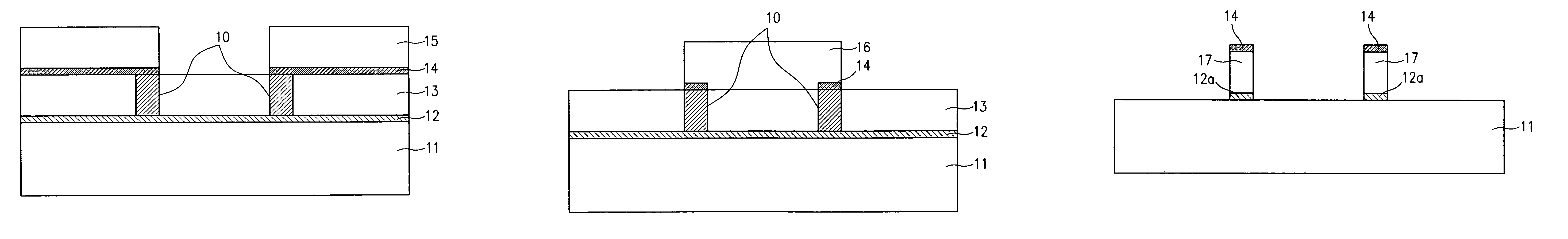
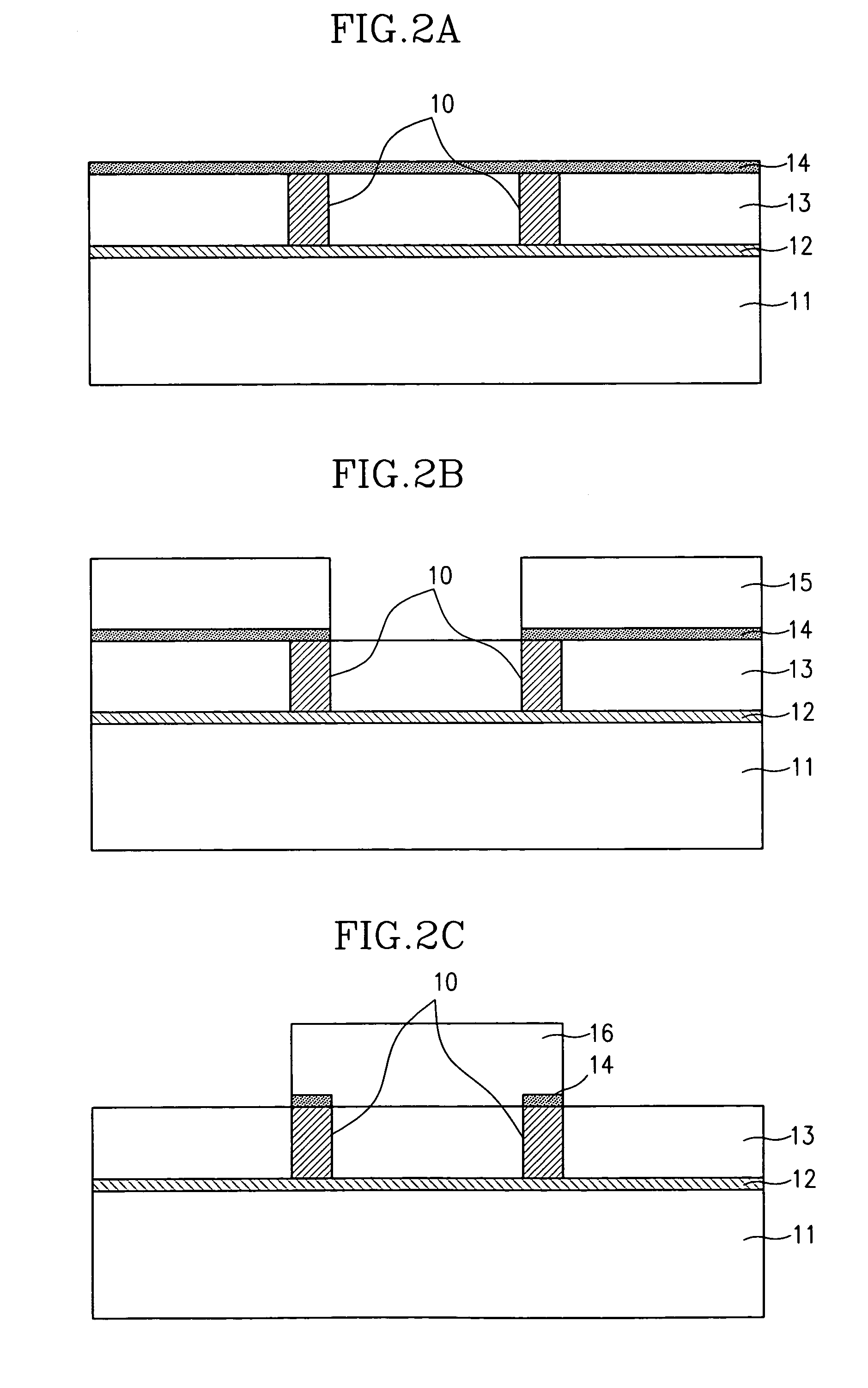
[0020]FIGS. 2A to 2E are sectional views showing a process of forming a gate electrode in a semiconductor device according to the present invention.

[0021]According to a method of forming a gate electrode according to the present invention, a line width of the gate electrode can be microscopically formed by performing a photolithography process twice.

[0022]One photolithography process is performed with a mask pattern which masks neighboring gate electrode areas and an area between the neighboring gate electrode areas. Another photolithography process is performed with a mask pattern which exposes the area between the neighboring gate electrode areas. And then, gate electrode etching is performed by the mask that is formed by a photolithography process twice.

[0023]To accomplish this, first, as shown in FIG. 2A, a gate oxide 12 is formed on a silicon substra...


PUM


Abstract

The present invention is directed to a method of forming a gate electrode in a semiconductor device, which is capable of reducing a line width of the gate electrode by performing a photolithography process after defining a wide region on which a gate electrode is located on a photoresist twice such that the line width of the gate electrode is not subject to a wavelength of a light source used when the photolithography process is performed. The method comprises forming a gate oxide on a semiconductor substrate, depositing a polysilicon on the gate oxide, forming a mask thin film on the polysilicon, patterning the mask thin film using a photolithography process twice, wherein one photolithography process is performed with a mask pattern which masks neighboring gate electrode areas and an area between the neighboring gate electrode areas, another photolithography process is performed with a mask pattern which exposes the area between the neighboring gate electrode areas, etching the polysilicon using the mask thin film pattern, and removing the mask thin film pattern on the polysilicon.

Description

BACKGROUND OF THE INVENTION[0001](a) Field of the Invention[0002]The present invention relates to a method of fabricating a semiconductor device, and more particularly to a method of forming a gate electrode in a semiconductor device, which is capable of reducing a line width of the gate electrode.[0003](b) Description of the Related Art[0004]With the development of manufacturing techniques for semiconductor devices and the expansion of their applications, research and development into increased integration of semiconductor devices has progressed rapidly. Also, with the increased integration of semiconductor devices, studies for downsizing semiconductors based on microscopic process technologies have progressed.[0005]With the downsizing of semiconductor devices, an adjustment of gate CD (critical dimension), which can be referred to as the width of gate, is very important. This is because a transistor driving current varies greatly depending on a variation of the gate CD.[0006]Conve...

Claims


Application Information

Patent Timeline
IPC IPC(8): H01L21/31H01L21/336H01L21/033H01L21/28H01L21/3205H01L21/3213H01L21/4763
CPCH01L21/0337H01L21/32139H01L21/28123H01L21/0338H01L21/18
Inventor PARK, GEON-OOK
Owner DONGBU ELECTRONICS CO LTD
Why Eureka
Try Eureka