Liquid crystal display device and method for manufacturing the same

a liquid crystal display and display device technology, applied in non-linear optics, instruments, optics, etc., can solve the problems of power consumption, limit in reducing the width of the gate line, and cannot adequately satisfy the present demands of display applications, etc., to achieve small area, reduce the width of the gate line, and high capacitance

Inactive Publication Date: 2008-12-30
LG DISPLAY CO LTD
View PDF10 Cites 4 Cited by
  • Summary
  • Abstract
  • Description
  • Claims
  • Application Information

AI Technical Summary

Benefits of technology

[0030]An advantage of the present invention is to provide an LCD device and a method for manufacturing the same in which a storage capacitor having high capacitance with a small area is formed to decrease a width of a gate line, thereby improving an aperture ratio and thus obtaining high picture quality.
[0031]Additional advantages and features of the invention will be set forth in part in the description which follows and in part will become apparent to those having ordinary skill in the art upon examination of the following or may be learned from practice of the invention. The objectives and other advantages of the invention may be realized and attained by the structure particularly pointed out in the written description and claims hereof as well as the appended drawings.
[0032]To achieve these and other advantages and in accordance with the purpose of the invention, as embodied and broadly described herein, an LCD device includes a first substrate defined by first and second regions; a storage capacitor electrode and a gate electrode respectively formed in the first and second regions of the first substrate; a gate insulating layer formed on an entire surface of the first substrate so that the first region is thinner than the second region; a semiconductor layer and source and drain electrodes deposited on the gate insulating layer of the second region, a conductive layer formed on the gate insulating layer of the first region; a pixel electrode electrically connected to the drain electrode and the conductive layer; a second substrate opposite to the first substrate; and an LC layer formed between the first and second substrates.
[0033]In another aspect of the present invention, a method for manufacturing an LCD device includes preparing a first substrate defined by first and second regions; forming a storage capacitor electrode in the first region of the first substrate; forming a gate electrode in the second region; forming a gate insulating layer on an entire surface of the first substrate so that the first region is thinner than the second region; forming a semiconductor layer and source and drain electrodes on the gate insulating layer of the second region, forming a conductive layer on the gate insulating layer of the first region; forming a pixel electrode electrically connected to the drain electrode and the conductive layer; and forming an LC between the first and second substrates opposite to each other.
[0034]In another embodiment of the present invention, a storage capacitor having a high capacitance with a small area is formed, so that a width of a gate line can be decreased compared with the related art, and an aperture ratio can be improved as much as the decreased width, thereby obtaining an LCD device of high picture quality.
[0035]It is to be understood that both the foregoing general description and the following detailed description of the present invention are exemplary and explanatory and are intended to provide further explanation of the invention as claimed.

Problems solved by technology

However, the CRT cannot adequately satisfy present demands for display applications that require reduced volume and weight, portability, and low power consumption while having a large screen size and high resolution.
However, the related art LCD device has the following problems.
However, since a desired capacitance cannot be obtained in a case of decreasing the width of the gate line, there was a limit in decreasing the width of the gate line.

Method used


Image

  • Liquid crystal display device and method for manufacturing the same
  • Liquid crystal display device and method for manufacturing the same
  • Liquid crystal display device and method for manufacturing the same

Examples


first embodiment

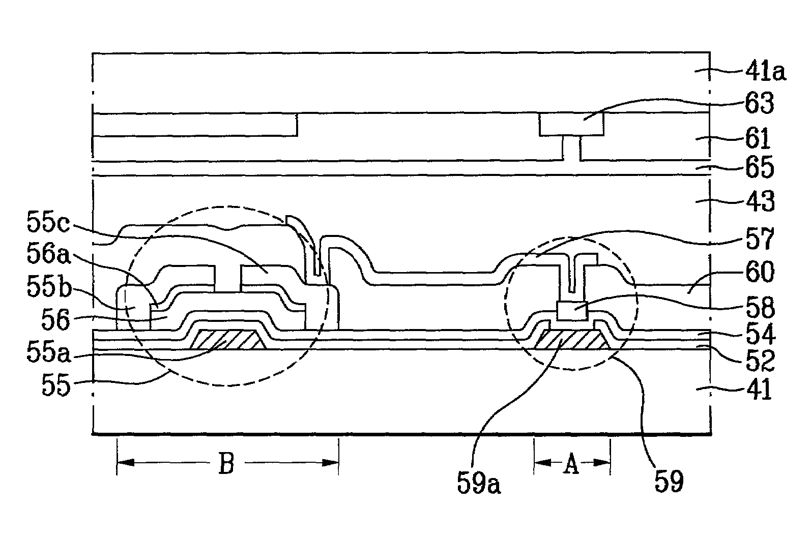
[0052]FIG. 4 is a sectional view of an LCD device according to the present invention, taken along line I-I′ of FIG. 3.

[0053]Referring to FIG. 4, the LCD device according to the first embodiment of the present invention includes a storage capacitor region (first region) and a TFT region (second region). As shown in FIG. 4, the LCD device includes a first substrate 41, a second substrate 41a, and an LC layer 43 formed between the two substrates. A storage capacitor 59 is formed in a first region A of the first substrate 41, and a TFT 55 is formed in a second region B of the first substrate 41.

[0054]Hereinafter, the first region A and the second region B will now be explained in more detail.

[0055]A gate electrode 55a for a TFT 55 and a storage capacitor electrode 59a spaced apart from the gate electrode 55a are formed on the first substrate 41.

[0056]A first insulating layer 52 is formed on an entire surface of the first substrate 41 except an upper portion of the storage capacitor elec...

second embodiment

[0085]A method for manufacturing the LCD device according to the present invention will be explained with reference to FIGS. 7A to 7D.

[0086]First, in the second embodiment of the present invention, another method for manufacturing an LCD device is proposed to obtain a high aperture ratio by making a gate insulating layer of a storage region thinner than a gate insulating layer of a TFT region.

[0087]As shown in FIG. 7A, a metal having low specific resistance such as Al, Cr, Cu, Mo, and Al alloy is formed by a sputtering method, and then the gate line (not shown), the gate electrode 55a, and the storage capacitor electrode 59a spaced apart from the gate electrode 55a are formed by a patterning process using a photo-lithography process etc. Subsequently, an insulating layer 71 is formed on the entire surface of the first substrate 41 including the storage capacitor electrode 59a. Then, as shown in FIG. 7B, the insulating layer 71 above the storage capacitor electrode 59a is etched at a...


PUM

PropertyMeasurementUnit
conductiveaaaaaaaaaa
widthaaaaaaaaaa
thicknessaaaaaaaaaa

Abstract

An LCD device and a method for manufacturing the same are disclosed, in which a width of a gate line is decreased by forming a storage capacitor of a high capacitance with a small area, and by improving an aperture ratio, thereby obtaining high picture quality.

Description

[0001]This application claims the benefit of Korean Patent Application No. 2000-84092 filed on Dec. 28, 2000, which is hereby incorporated by reference as if fully set forth herein.BACKGROUND OF THE INVENTION[0002]1. Field of the Invention[0003]The present invention relates to a liquid crystal display (LCD) device, and more particularly, to an LCD device and a method for manufacturing the same.[0004]2. Discussion of the Related Art[0005]Rapid development within the fields of information and communication has caused an increase in the demand for thin, lightweight and low cost display devices for viewing information. Industries that develop displays are responding to these needs by placing a high emphasis on developing flat panel type displays.[0006]Historically, the Cathode Ray Tube (CRT) has been widely used as a display device in applications such as televisions, computer monitors, and the like, because CRT screens can display various colors having high luminance. However, the CRT ...

Claims


Application Information

Patent Timeline
Patent Type & Authority Patents(United States)
IPC IPC(8): G02F1/1343G02F1/136G02F1/1362
CPCG02F1/136213G02F1/136
Inventor YOO, HONG SUKKIM, WOO HYUN
Owner LG DISPLAY CO LTD
Why Eureka
Try Eureka