Shielded gate trench mosfet with ESD diode manufactured using two poly-silicon layers process

a technology of shielded gate trench and polysilicon layer, which is applied in the direction of diodes, semiconductor devices, electrical devices, etc., can solve the problems of high fabrication cost, dynamic avalanching instability, complicated manufacturing process, etc., and achieve the effect of reducing the width of shielded gate and increasing switching loss

Active Publication Date: 2021-04-08
NAMI MOS CO LTD
View PDF0 Cites 6 Cited by
  • Summary
  • Abstract
  • Description
  • Claims
  • Application Information

AI Technical Summary

Benefits of technology

[0007]The present invention provides a SGT trench MOSFET having an ESD clamp diode and requiring only two poly-silicon layers, moreover, the present invention has n type doped poly-silicon as the shielded gate which means the invented device can be shrunk with reducing shielded gate width for Rds reduction without increasing switching loss and having dynamic switching instability.

Problems solved by technology

However, the SGT MOSFET in FIG. 1B requires three poly-silicon layers (one poly-silicon layer for the shielded electrode, another for trenched gate and the other for ESD diode) and two mask layers for the shielded gate and the ESD diode, respectively, resulting in a complicated manufacture process and causing a high fabrication cost.
The high shielded gate resistance will induce dynamic avalanching instability and more switching loss due to the shielded gate served as the snubber.

Method used


Image

  • Shielded gate trench mosfet with ESD diode manufactured using two poly-silicon layers process
  • Shielded gate trench mosfet with ESD diode manufactured using two poly-silicon layers process
  • Shielded gate trench mosfet with ESD diode manufactured using two poly-silicon layers process

Examples


Embodiment Construction

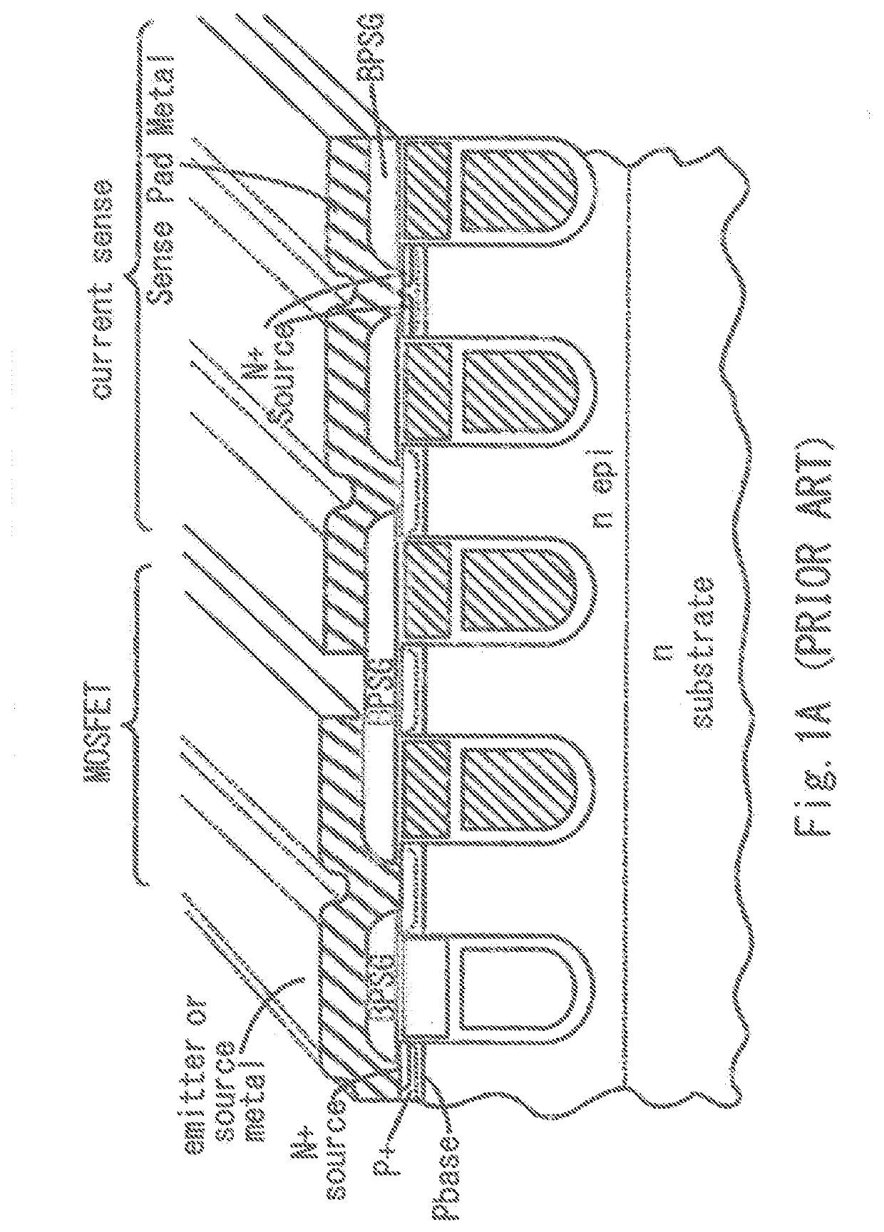
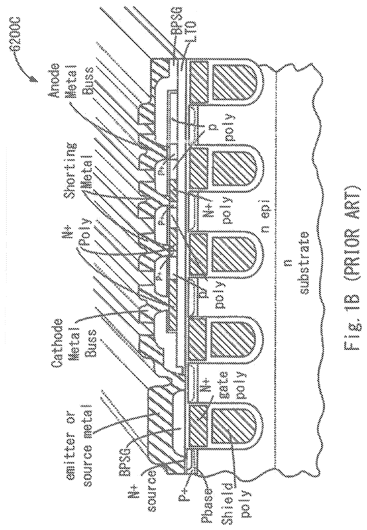
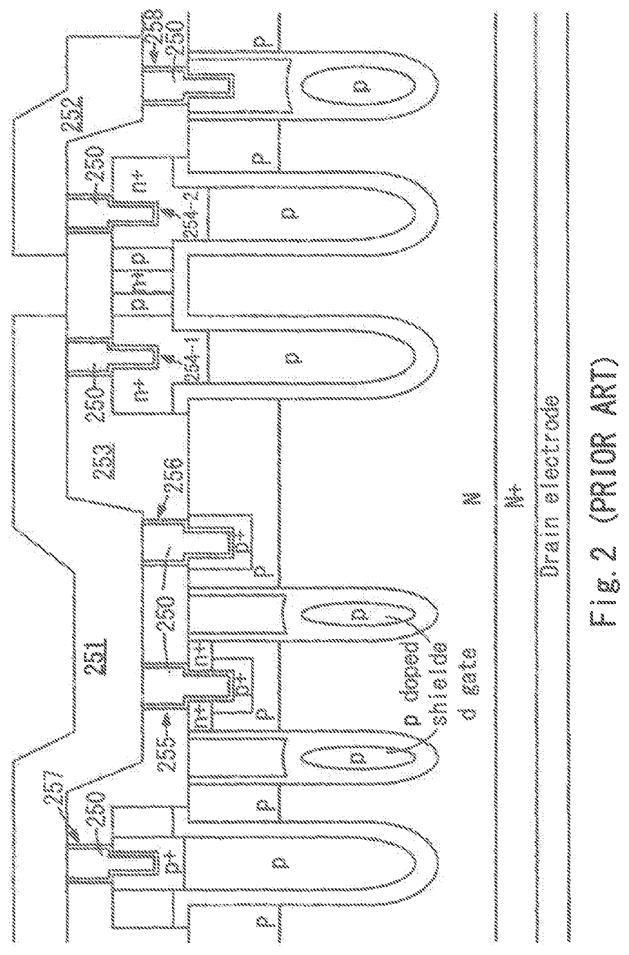
[0025]In the following Detailed Description, reference is made to the accompanying drawings, which forms a part thereof, and in which is shown by way of illustration specific embodiments in which the invention may be practiced. In this regard, directional terminology, such as “top”, “bottom”, “front”, “back”, etc., is used with reference to the orientation of the Figure(s) being described. Because components of embodiments can be positioned in a number of different orientations, the directional terminology is used for purpose of illustration and is in no way limiting. It is to be understood that other embodiments may be utilized and structural or logical changes may be made without departing from the scope of the present invention. The following detailed description, therefore, is not to be taken in a limiting sense, and the scope of the present invention is defined by the appended claims, it is to be understood that the features of the various exemplary embodiments described herein...


PUM

PropertyMeasurementUnit
conductivityaaaaaaaaaa
thicknessaaaaaaaaaa
conductivity typeaaaaaaaaaa

Abstract

A SGT MOSFET having ESD diode and a method of manufacturing the same are disclosed. The SGT trench MOSFET according to the present invention, has n+ doped shielded electrode in an N channel device and requires only two poly-silicon layers, making the device can be shrunk with reducing shielded gate width for Rds reduction without increasing switching loss and having dynamic switching.

Description

FIELD OF THE INVENTION[0001]This invention relates generally to semiconductor devices, and more particularly, to a shielded gate trench MOSFET (Metal Oxide Semiconductor Field Effect Transistor) with ESD diode and a manufacturing process using only two poly-silicon layers.BACKGROUND OF THE INVENTION[0002]Please refer to FIG. 1A for a shielded gate trench MOSFET (SGT) of prior art disclosed in U.S. Pat. No. 7,855,415. Compared to a conventional trench MOSFET having single trenched gate, a shielded gate trench MOSFET as shown in FIG. 1A is more attractive due to its reduced Cgd (capacitance between gate and drain) in accordance with reduced Qgd (charge between gate and drain), and increased breakdown voltage of the trench MOSFET, making an excellent choice for power switching applications such as inverter and DC to DC power supply circuits. Moreover, the SGT has a shielded gate as a built-in RC snubber which is important for suppressing EMI (electromagnetic interface). Furthermore, in...

Claims


Application Information

Patent Timeline
Patent Type & Authority Applications(United States)
IPC IPC(8): H01L27/02H01L29/66H01L29/78H01L29/423H01L29/40
CPCH01L27/0255H01L29/66734H01L29/401H01L29/7808H01L29/4236H01L29/7813H01L29/66704H01L29/7821H01L29/7825H01L29/0634H01L29/45H01L29/4175H01L29/407H01L29/41766H01L29/404H01L29/0619H01L29/66727
Inventor HSIEH, FU-YUAN
Owner NAMI MOS CO LTD
Why Eureka
Try Eureka