Solid state imaging device and method for manufacturing the same

a solid-state imaging and imaging device technology, applied in the direction of diodes, semiconductor devices, radiation controlled devices, etc., can solve the problems of rts noise, s/n characteristic of the circuit may deteriorate, and the number of carriers n decreases, so as to improve s/n characteristic of the circuit, suppress the occurrence of rts noise, and high sensitive

Active Publication Date: 2009-11-26
PANASONIC SEMICON SOLUTIONS CO LTD
View PDF3 Cites 20 Cited by
  • Summary
  • Abstract
  • Description
  • Claims
  • Application Information

AI Technical Summary

Benefits of technology

[0027]According to the present disclosure described above, even when the gate width of the amplifying transistor isolated by the STI region is reduced as the size of the pixel cells is reduced, the number of carriers of the amplifying transistor can be increased, and the occurrence of the RTS noise can be suppressed. As a result, the S / N characteristic of the circuit can be improved. This allows manufacture of high sensitive solid state imaging devices with high yield.
[0028]Thus, the present disclosure advantageously makes it possible to manufacture the high sensitive solid state imaging devices with stability, and is useful for solid state imaging devices and methods for manufacturing the same.

Problems solved by technology

As expressed by the equation (1), when the size of the amplifying transistors is reduced due to the size reduction of the pixel cells, the number of carriers N decreases, and the RTS noise is likely to occur.
As a result, an S / N characteristic of the circuit may deteriorate.

Method used


Image

  • Solid state imaging device and method for manufacturing the same
  • Solid state imaging device and method for manufacturing the same
  • Solid state imaging device and method for manufacturing the same

Examples


embodiment

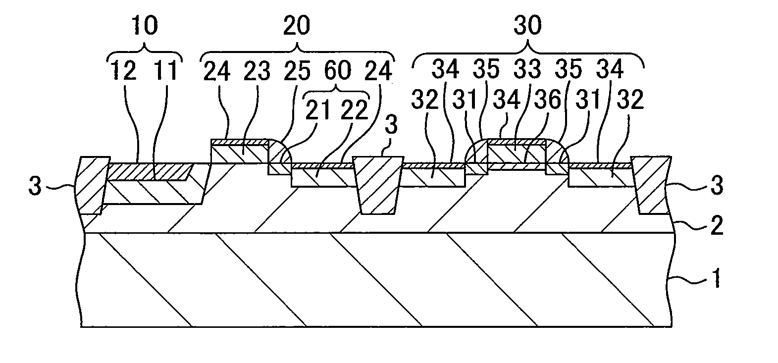
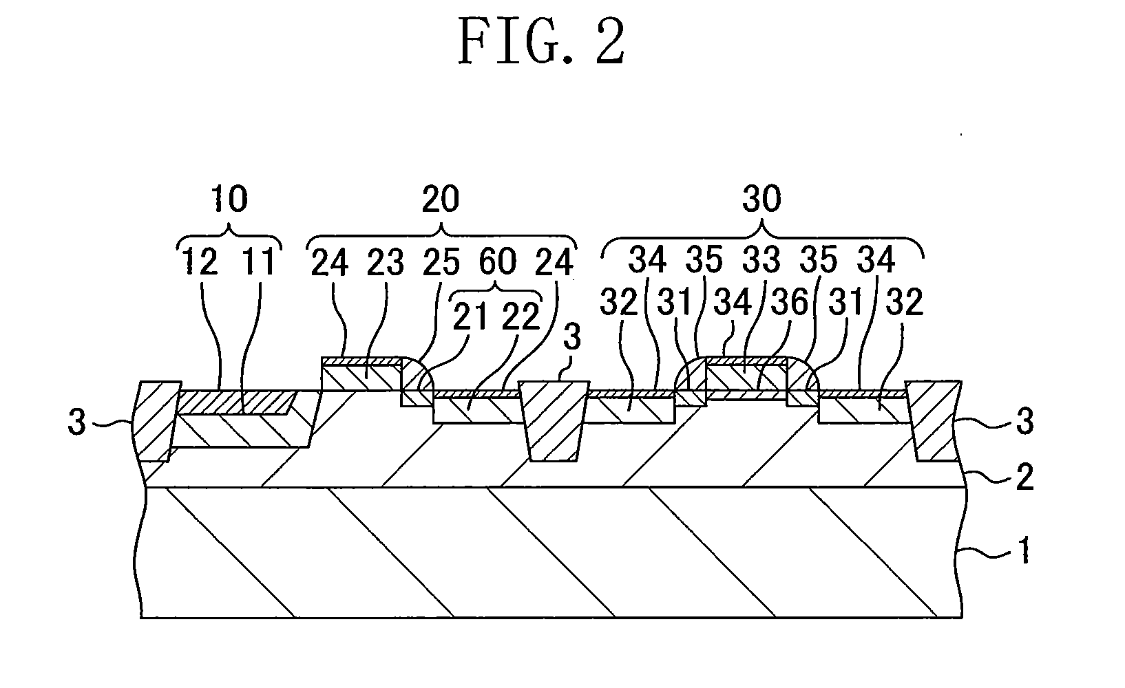
[0038]Hereinafter, an example solid state imaging device and an example method for manufacturing the same according to the present disclosure will be explained with reference to the drawings.

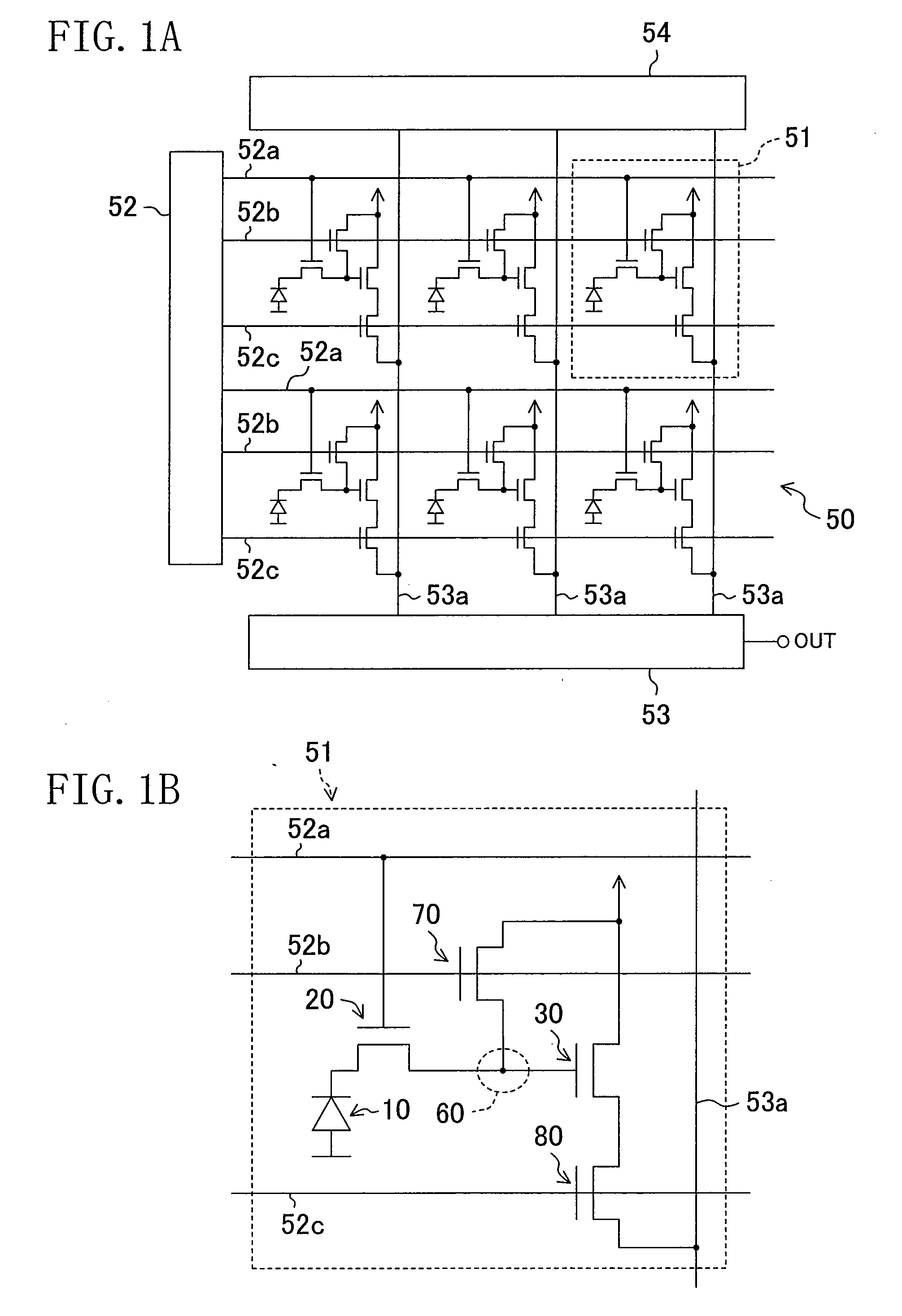
[0039]FIG. 1A is a circuit diagram schematically illustrating the structure of a first example solid state imaging device, more specifically, a MOS solid state imaging device. FIG. 1B is a circuit diagram illustrating an enlargement of one of unit pixels shown in FIG. 1A. As shown in FIG. 1A, a light sensitive region 50 of the example MOS solid state imaging device includes a plurality of unit pixels 51 arranged in a two-dimensional array. A peripheral circuit including, for example, a vertical shift register 52 for selecting the pixels in a column direction, a horizontal shift register 53 for selecting the pixels in a line direction, and a pulse generator circuit 54 for supplying a timing pulse to the vertical shift register 52 and the horizontal shift register 53, is formed around the light se...


PUM


Abstract

A solid state imaging device includes a transfer transistor for transferring signal charges generated by photoelectric conversion to a floating diffusion layer, a reset transistor for resetting a potential of the floating diffusion layer, and an amplifying transistor for outputting a signal corresponding to the potential of the floating diffusion layer. A low concentration impurity region having an impurity concentration lower than that of the first conductivity type semiconductor region is formed in part of a surface portion of the first conductivity type semiconductor region which is located below a gate electrode of the amplifying transistor and serves as a well region of the amplifying transistor.

Description

CROSS-REFERENCE TO RELATED APPLICATION[0001]This non-provisional application claims priority under 35 U.S.C. §119(a) of Japanese Patent Application No. 2008-133884 filed in Japan on May 22, 2008, the entire contents of which are hereby incorporated by reference.BACKGROUND OF THE INVENTION[0002]The present disclosure relates generally to solid state imaging devices used in digital still cameras and the like and methods for manufacturing the same.[0003]MOS (Metal Oxide Semiconductor) solid state imaging devices, including a MOS transistor for amplifying a signal detected by a photodiode in each pixel, have higher sensitivity as compared with CCD (Charge Coupled Device)-type solid state imaging devices.[0004]FIG. 8 is a sectional view schematically illustrating the structure of a unit pixel and an amplifying transistor of a conventional MOS solid state imaging device. In FIG. 8, a photodiode and a transfer transistor are shown as the unit pixel. The structure of the amplifying transfer...

Claims


Application Information

Patent Timeline
Patent Type & Authority Applications(United States)
IPC IPC(8): H01L27/148H01L21/322
CPCH01L27/14609H01L27/14643H01L27/14689H01L27/14612H01L29/665H01L29/6659H01L29/7833H01L29/105
Inventor TSUNO, MORIKAZU
Owner PANASONIC SEMICON SOLUTIONS CO LTD
Why Eureka
Try Eureka