Lead frame and method of manufacturing the same

a technology of lead frame and manufacturing method, which is applied in the field of lead frame, can solve the problems of environmental problems, defect in semiconductor chips, and laborious and troublesome working steps in the process of solvent plating, and achieve the effect of increasing the density of the plating layer

Active Publication Date: 2007-09-11
HAESUNG CO LTD
View PDF16 Cites 0 Cited by
  • Summary
  • Abstract
  • Description
  • Claims
  • Application Information

AI Technical Summary

Benefits of technology

[0022]The present invention is directed to a lead frame having a structure capable of reducing a galvanic potential difference between plating layers, and to a method of manufacturing the lead frame.
[0023]The present invention also provides a lead frame, and a method of manufacturing the lead frame, that can discharge hydrogen to the outside which is adsorbed in the plating layer during plating of the layer, and thus reducing air pockets and related defects in the layer.
[0033]According to the present invention, the lead frame having can restrict a surface of the lead frame from corrosion since density of the plating layer can be increased and other defects discussed above in association with the conventional lead frames can be substantially reduced.

Problems solved by technology

However, the soldering base plating in the semiconductor packaging process has several known drawbacks.
For example, the soldering plating process requires tedious and troublesome working steps.
Also, the lead components on the exposed lead and the lead plating solution can cause environmental problems.
Moreover, the plating solution can penetrate into a gap between the surface of the lead frame and the epoxy molding, and often causes defects in the semiconductor chips.
In addition, an additional process for correcting a non-uniformity in the plating layer is often required.
However, when plating the lead frame 120, if defects exist on the surface of the base metal layer 121 in spite of a pre-treatment, the Ni plating progresses more rapidly on the defect regions than other regions since the surface energy in the defect regions is greater than other regions, thereby resulting in a rough plating surface on the defect regions and a poor adhesion due to the unbalance in the plating over the plating surface.
However, cracks can form in the plating texture surface during the subsequent packaging or handling processes of the semiconductor device.
Consequently, this peeled surface can be subject to corrosion because of a galvanic potential difference caused by the exposure of the plating layers to the air.
Accordingly, a severe corrosion can be caused by a galvanic coupling due to the dielectric difference.
In particular, as depicted in FIG. 3, cracks or defects can easily occur in the lead frame during the manufacturing process, and the protective plating layer 124 can be peeled off because of the cracks or the defects.
Therefore, the corrosion problem due to formation of the galvanic coupling on the exposed area 120c still remains.

Method used


Image

  • Lead frame and method of manufacturing the same
  • Lead frame and method of manufacturing the same
  • Lead frame and method of manufacturing the same

Examples


Embodiment Construction

[0046]The present invention will now be described more in details with reference to the accompanying drawings in which exemplary embodiments of the invention are shown.

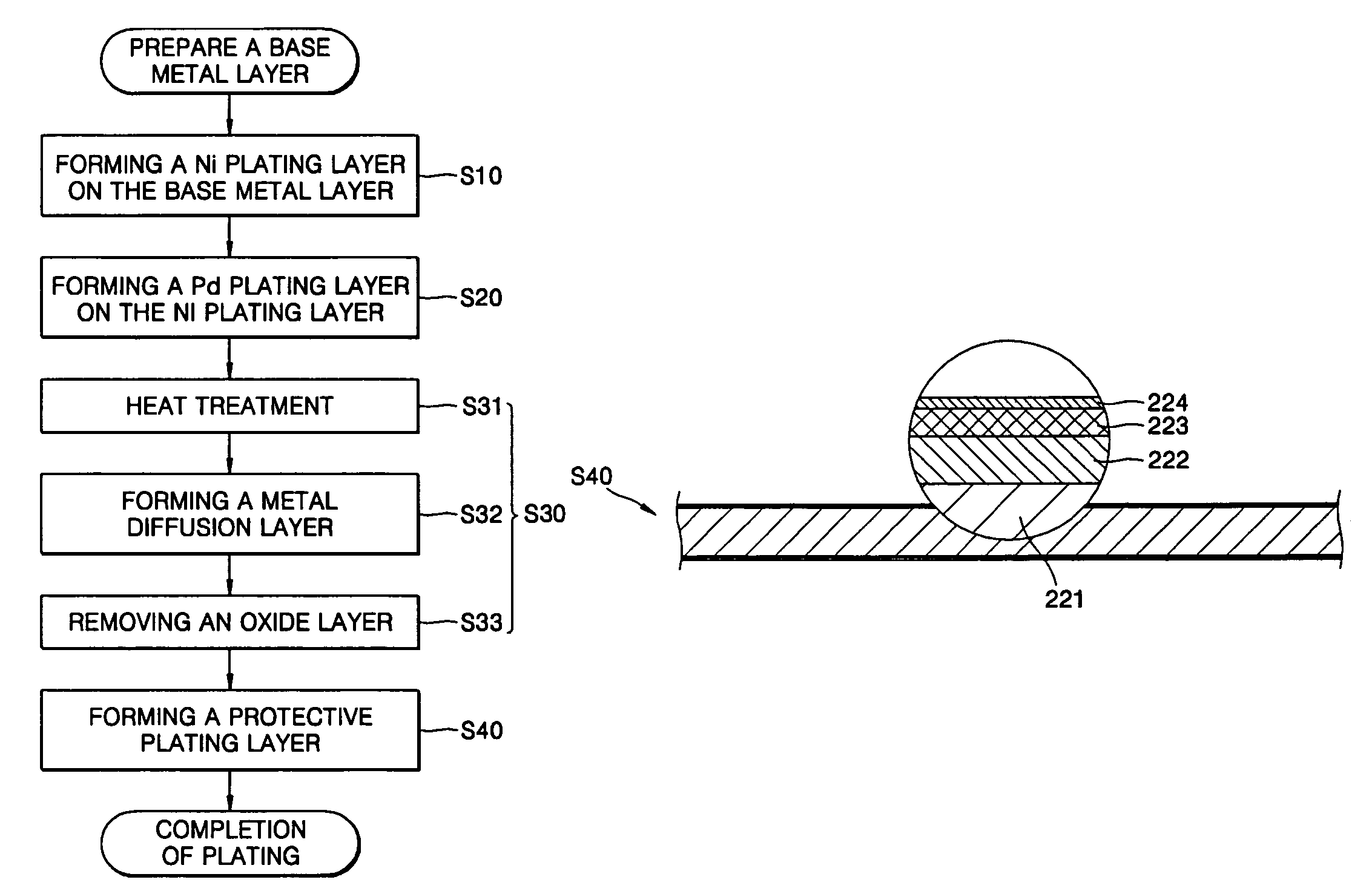
[0047]FIG. 4 is a flow chart illustrating a method of manufacturing the lead frame according to one embodiment of the present invention. FIGS. 5A through 5D are partial and cross-sectional views illustrating a process and construction of the lead frame according to one embodiment of the present invention. By the process, plating layers are formed on a base metal layer of the lead frame prior to packaging of the semiconductor chip with the lead frame.

[0048]Referring to FIGS. 4, and 5A-5D, a base metal layer 221 is provided in the form of a bare frame for the lead frame. The base metal layer 221 is formed of a suitable metal known in the art, such as copper or alloy 42.

[0049]A Ni plating layer 222 is formed thereon by plating Ni or a Ni alloy on a surface of the base metal layer 221 (S10). The Ni plating layer 222 preve...


PUM

PropertyMeasurementUnit
temperatureaaaaaaaaaa
timeaaaaaaaaaa

Abstract

A lead frame having a structure that can discharge hydrogen adsorbed during deposition and can reduce a galvanic potential difference between plating layers and a method of manufacturing the same are provided. The method includes forming a Ni plating layer formed of Ni or a Ni alloy on a base metal layer formed of a metal, forming a Pd plating layer formed of Pd or an Pd alloy on the Ni plating layer, heat-treating the Ni plating layer and the Pd plating layer, and forming a protective plating layer on the heat-treated Pd plating layer.

Description

BACKGROUND OF THE INVENTION[0001]This application claims the priority of Korean Patent Application No. 2004-26204, filed on Apr. 16, 2004, in the Korean Intellectual Property Office, the disclosure of which is incorporated herein in its entirety by reference.FIELD OF THE INVENTION [0002]The present invention relates to a lead frame for a semiconductor device and to a method of manufacturing the lead frame.DESCRIPTION OF THE RELATED ART[0003]A lead frame is a structural element forming a semiconductor package with a semiconductor chip mounted thereon, and performs as a lead for connecting the semiconductor package to an external device and as a frame for supporting the semiconductor chip.[0004]FIG. 1 is a plan view of a typical lead frame 100 that comprises a die pad 110 and plural leads 120 arranged about the die pad 110. The die pad 110 connects to a side rail 170 at the four corners by a pad supporting lead 180, and supports a semiconductor chip mounted thereon.[0005]The lead 120 ...

Claims


Application Information

Patent Timeline
Patent Type & Authority Patents(United States)
IPC IPC(8): H01L23/495B32B15/01B32B15/20C25D5/48C23C30/00C25D7/12H01L21/44H01L21/50H01L23/48H01L23/50
CPCH01L23/49582H01L24/48Y10T428/12903H01L2224/45144H01L2224/48091H01L2224/48247H01L2224/48599H01L2224/49171H01L2224/85464H01L2924/01004H01L2924/01006H01L2924/01007H01L2924/01011H01L2924/01015H01L2924/01016H01L2924/01018H01L2924/01022H01L2924/01027H01L2924/01028H01L2924/01029H01L2924/01033H01L2924/01046H01L2924/01047H01L2924/0105H01L2924/01052H01L2924/01075H01L2924/01078H01L2924/01079H01L2924/01082H01L2924/014Y10T428/12528Y10T428/12889Y10T428/1291Y10T428/12875H01L24/49H01L24/45H01L2924/00014H01L2924/00H01L2224/48664H01L2924/12042H01L2924/181H01L2924/00012H01L23/48
Inventor PAEK, SUNG-KWANPARK, SE-CHUELLEE, SANG-HUN
Owner HAESUNG CO LTD
Why Eureka
Try Eureka