Method and apparatus for specimen fabrication

a technology of method and apparatus, applied in the field of method and apparatus specimen fabrication, can solve the problems of poor processing, deterioration of profit, and decrease in manufacturing yield, and achieve the effect of increasing the throughput of sample preparation and saving the time necessary

Inactive Publication Date: 2007-09-11
HITACHI LTD
View PDF21 Cites 28 Cited by
  • Summary
  • Abstract
  • Description
  • Claims
  • Application Information

AI Technical Summary

Benefits of technology

[0028]According to the invention, the sample fabricating method for analyzing, observing, or measuring a micro area by separating a micro sample including a requested specific area from a sample of an electronic part such as a semiconductor wafer, a semiconductor device, or the like or preparing the micro sample without tilting a specimen stage can be realized. Particularly, by setting the FIB irradiation angle in the range from 30 degrees to 75 degrees, the surface of the sample can be observed excellently, and the shape of the micro sample is formed to be suitable for fabrication.
[0072](27) In the sample fabricating apparatus in any of (21) to (26), an input apparatus for setting a requested-section depression angle of a requested section or a parameter equivalent to the requested-section depression angle is provided. With the configuration, the operator can easily set the depression angle of the requested section.

Problems solved by technology

Electronic parts such as a semiconductor memory typified by a dynamic random access memory, a microprocessor, a semiconductor device such as a semiconductor laser, and a magnetic head are required to be manufactured in a high yield since decrease in the manufacturing yield due to occurrence of a defect causes profit deterioration.
Consequently, early detection / measure of / against a defect, a foreign matter, and poor processing as causes of a failure are big tasks.
However, as the packing density of a semiconductor device is becoming higher, an object cannot be observed with the resolution of the SEM.
However, it increases the price of the wafer itself, an added value increases as the manufacturing process advances and, further, the number of semiconductor devices lost by discarding a wafer increases.
Therefore, the conventional test method accompanying cutting of the wafer is very uneconomical.
However, the actually formed section is not perfectly perpendicular to the surface of a sample due to flare of a processing beam and re-deposition of a sputtered substance, and a slight taper exists.
The conventional methods have the following problems.
Consequently, a problem such that it takes time to tile a large stage with high accuracy and, as a result, sample fabrication time becomes longer arises.
Due to heavy weight of the specimen stage itself, the eucentric is not maintained before and after the tilting and the sample position relative to the ion beam irradiating optical system moves, so that the focal point of the FIB is relatively largely deviated from the surface of the sample, the surface of the sample cannot be observed, and a problem such that the ion beam irradiating optical system has to be re-adjusted also occurs.
However, by the above-described conventional methods, fabrication of a sample for analyzing, observing or measuring a micro area by separating a micro sample from an original sample (wafer) or preparing the micro sample to be separated cannot be realized.
However, according to the conventional methods, it is difficult to emit an FIB at an arbitrary angle.
Consequently, it is difficult to eliminate the taper.

Method used


Image

  • Method and apparatus for specimen fabrication
  • Method and apparatus for specimen fabrication
  • Method and apparatus for specimen fabrication

Examples


first embodiment

[0107]A schematic configuration of a sample fabricating apparatus as an embodiment of the invention will be describe by referring to FIG. 4.

[0108]A sample fabricating apparatus 17 has a vacuum chamber 41 in which an ion beam irradiating optical system 35 constructed by an ion source 32, a beam limiting aperture 33, an ion beam scanning electrode 34, an ion beam lens 31, and the like; a secondary electron detector 36 for detecting secondary electrons and secondary ions emitted from a sample irradiated with an FIB; a deposition-gas supplying source 37 for supplying an original material gas to form a deposition film in an ion beam irradiation area; the probe 3 attached at the tip of a manipulator 42; a specimen stage 39 on which a specimen base 38 such as a semiconductor wafer or a semiconductor chip is placed; a sample holder 40 for fixing a micro sample as a part extracted from the specimen base 38, and the like are disposed. In this case, the ion beam irradiating optical system 35 i...

second embodiment

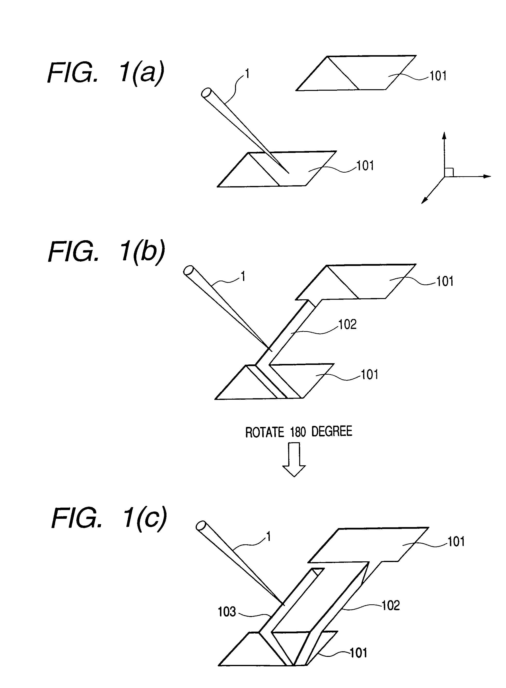
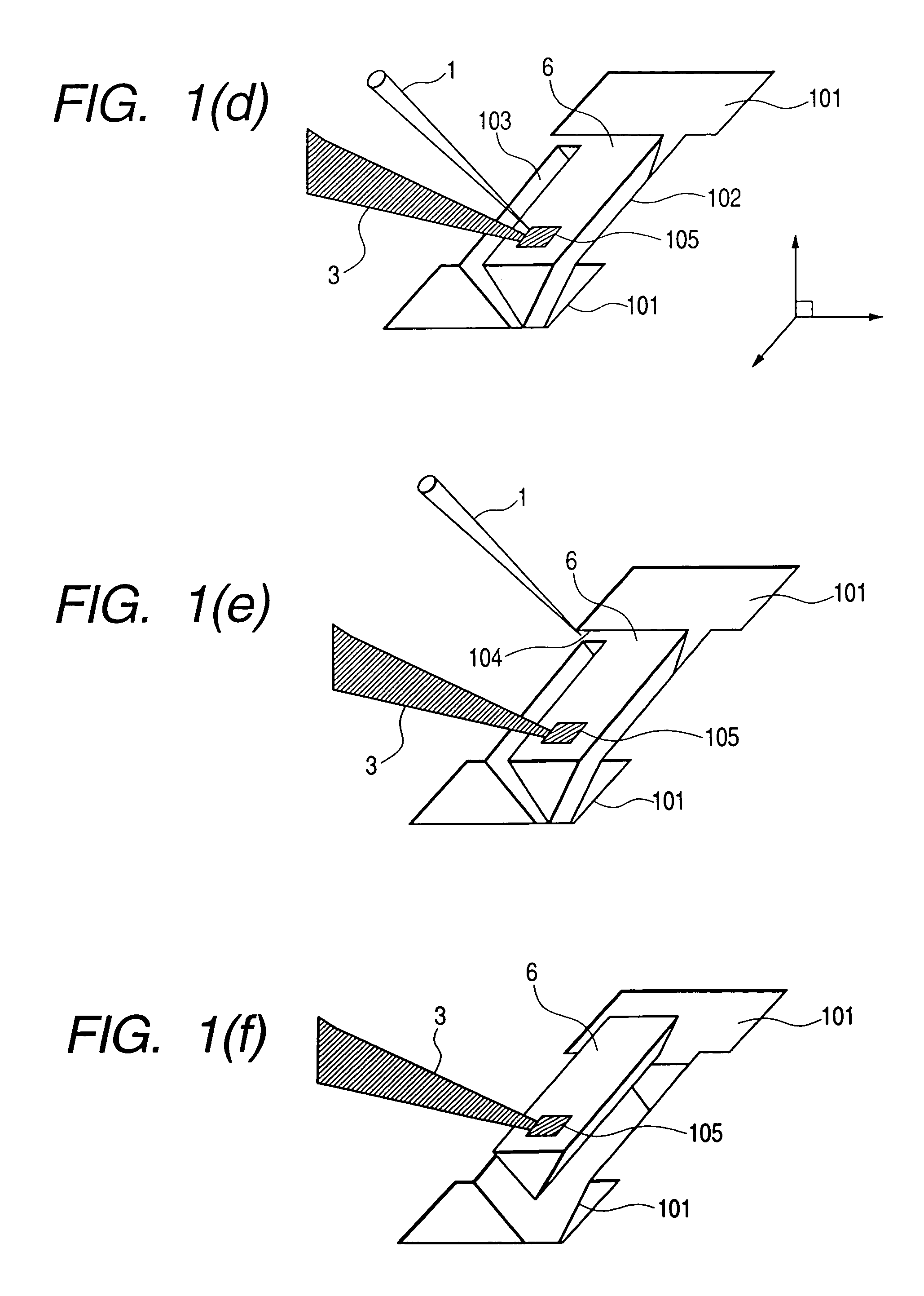
[0123]Another sample fabricating method as an embodiment of the invention will now be described by referring to FIGS. 6(a) to 6(d). A sample fabricating apparatus similar to the apparatus shown in FIG. 4 is used.

[0124]First, a mark indicative of the fabrication position of a membrane for TEM observation and a protection film are formed on a specimen base. A rectangle whose one side is in the direction of projection of the irradiation axis of an FIB to the base surface onto the surface of the sample is scanned with the FIB 1 on the specimen base to form two rectangular holes 301 (FIG. 6(a)) having a depth of about 15 μm and tapered in the depth direction. In this case, a membrane between the two rectangular holes 301 is a sample as a target and the thickness of the membrane is about 100 nm. Subsequently, membrane both ends 302 are cut. By using the axis perpendicular to the surface of the sample as a rotation axis, the sample is turned by about 90 degrees. By performing an image proc...

third embodiment

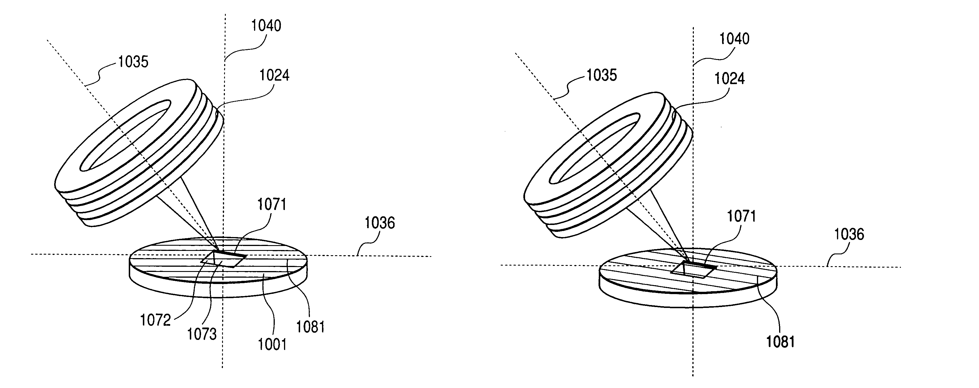
[0129]FIG. 7 is a schematic configuration diagram of a sample fabricating apparatus having an electron beam irradiating apparatus as an embodiment of the invention. A sample fabricating apparatus 17 has a vacuum chamber 41 in which an ion beam irradiating optical system 35, a secondary electron detector 36, a deposition-gas supplying source 37, a probe 3, a specimen stage 39, and the like are disposed in a manner similar to the sample fabricating apparatus of the second embodiment. Similarly, the ion beam irradiating optical system 35 is mounted relative to the stage 39 so that the angle formed between the FIB optical axis and the surface of the sample becomes 45 degrees. The specimen stage has the function of turning around a line segment perpendicular to the surface of a sample as a rotation axis. In the apparatus, an electron beam irradiating system constructed by a field emission electron gun 81 for emitting an electron beam, an electron beam lens 82, an electron scanning electr...


PUM

PropertyMeasurementUnit
angleaaaaaaaaaa
angleaaaaaaaaaa
gradient angleaaaaaaaaaa

Abstract

A sample fabricating method of irradiating a sample with a focused ion beam at an incident angle less than 90 degrees with respect to the surface of the sample, eliminating the peripheral area of a micro sample as a target, turning a specimen stage around a line segment perpendicular to the sample surface as a turn axis, irradiating the sample with the focused ion beam while the incident angle on the sample surface is fixed, and separating the micro sample or preparing the micro sample to be separated. A sample fabricating apparatus for forming a sample section in a sample held on a specimen stage by scanning and deflecting an ion beam, wherein an angle between an optical axis of the ion beam and the surface of the specimen stage is fixed and formation of a sample section is controlled by turning the specimen stage.

Description

CROSS-REFERENCE TO RELATED APPLICATIONS[0001]This application is a Continuation application of U.S. application Ser. No. 10 / 699,853 filed on Nov. 4, 2003, now U.S. Pat. No. 6,794,663 which is a Continuation application of U.S. application Ser. No. 09 / 985,537 filed on Nov. 5, 2001 now U.S. Pat. No. 6,664,552. Priority is claimed based on U.S. application Ser. No. 10 / 699,853 filed on Nov. 4, 2003, which claims the priority date of U.S. application Ser. No. 09 / 985,537 filed on Nov. 5, 2001, which claims the priority dates of Japanese applications 2000-342372 and 2001-204768 filed on Nov. 6, 2000 and Jul. 5, 2001, respectively.BACKGROUND OF THE INVENTION[0002]The present invention relates to method and apparatus specimen fabrication for analyzing, observing, or measuring a micro area by separating a micro sample including a requested specific area from a sample of an electronic part such as a semiconductor wafer or a device or preparing the micro sample to be separated by using a focuse...

Claims


Application Information

Patent Timeline
Patent Type & Authority Patents(United States)
IPC IPC(8): G21G5/00B23K15/00G01N1/28G01N23/20G01Q20/02G01Q30/20G01Q70/00
CPCB23K15/0006B23K15/0013G01N23/20G01N1/286H01J2237/31745H01J2237/3114
Inventor SHICHI, HIROYASUISHITANI, TOHRUKOIKE, HIDEMIUMEMURA, KAORUSEYA, EIICHITOKUDA, MITSUOTOMIMATSU, SATOSHIKASHIMA, HIDEOFUKUDA, MUNEYUKI
Owner HITACHI LTD
Why Eureka
Try Eureka