Divisible true dual port memory system supporting simple dual port memory subsystems

a dual-port memory and sub-system technology, applied in the field of memory systems, can solve the problems that the conventional sram system cannot be effectively divided into several sram sub-systems, and achieve the effects of low block count, high bit density, and low block coun

Inactive Publication Date: 2007-09-11
ALTERA CORP
View PDF3 Cites 3 Cited by
  • Summary
  • Abstract
  • Description
  • Claims
  • Application Information

AI Technical Summary

Benefits of technology

[0010]Many benefits are achieved by way of the present invention over conventional techniques. For example, some embodiments of the present invention provide an M-bit width and N-bit size TDP / SDP memory block that can be used as two independent M-bit width and N / 2-bit size SDP memory blocks. Certain embodiments of the present invention provide flexibility to a memory system. For a given memory area, the number of memory blocks and the bit density is often a tradeoff. For example, an embedded memory structure with large memory blocks often has a high bit density but a low block count. In contrast, an embedded memory with small memory blocks often has a low bit density but a high block count. Some embodiments of the present invention can satisfy different memory demands in FPGA applications. For example, some applications need large memory blocks with low block count. In contrast, other applications need small memory blocks with high block count. Depending on the applications, the M-bit width and N-bit size memory can be used as a single block for TDP or SDP operations, or used as two independent blocks for SDP operations. Certain embodiments of the present invention provide configurable memory block in FPGA fabric that supports a configurable data width and various operation modes including TDP, SDP and Single Port (SP) mode.

Problems solved by technology

The conventional SRAM system usually cannot be divided effectively into several SRAM sub-systems.

Method used


Image

  • Divisible true dual port memory system supporting simple dual port memory subsystems
  • Divisible true dual port memory system supporting simple dual port memory subsystems
  • Divisible true dual port memory system supporting simple dual port memory subsystems

Examples


Embodiment Construction

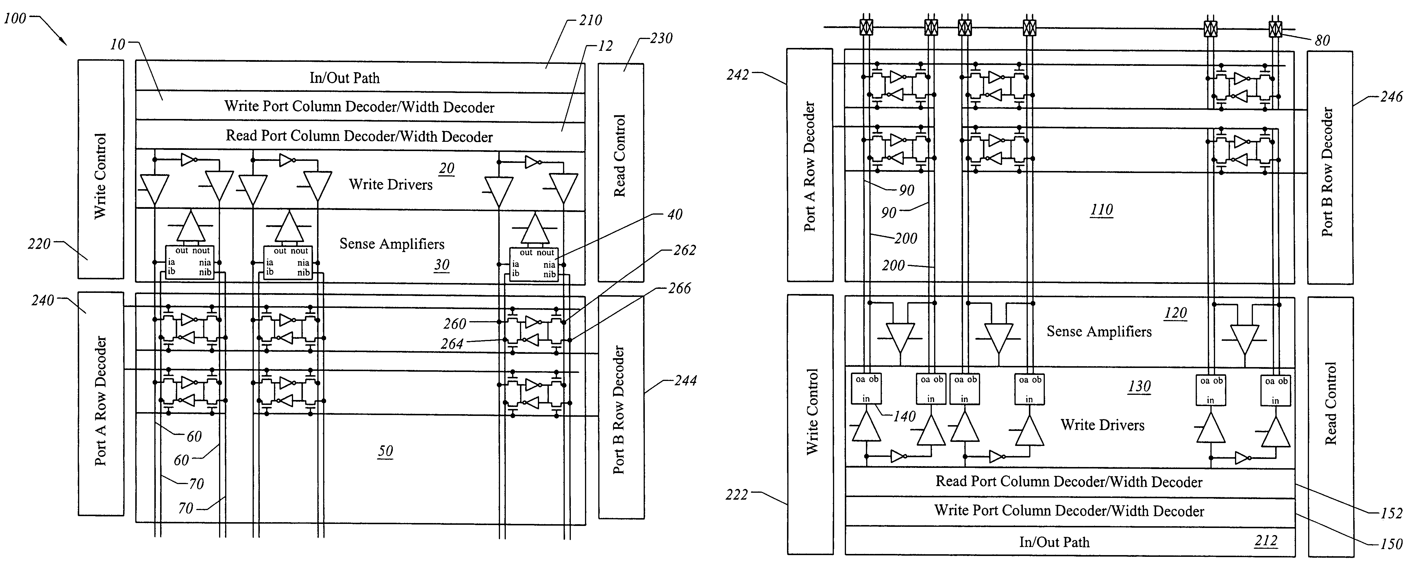
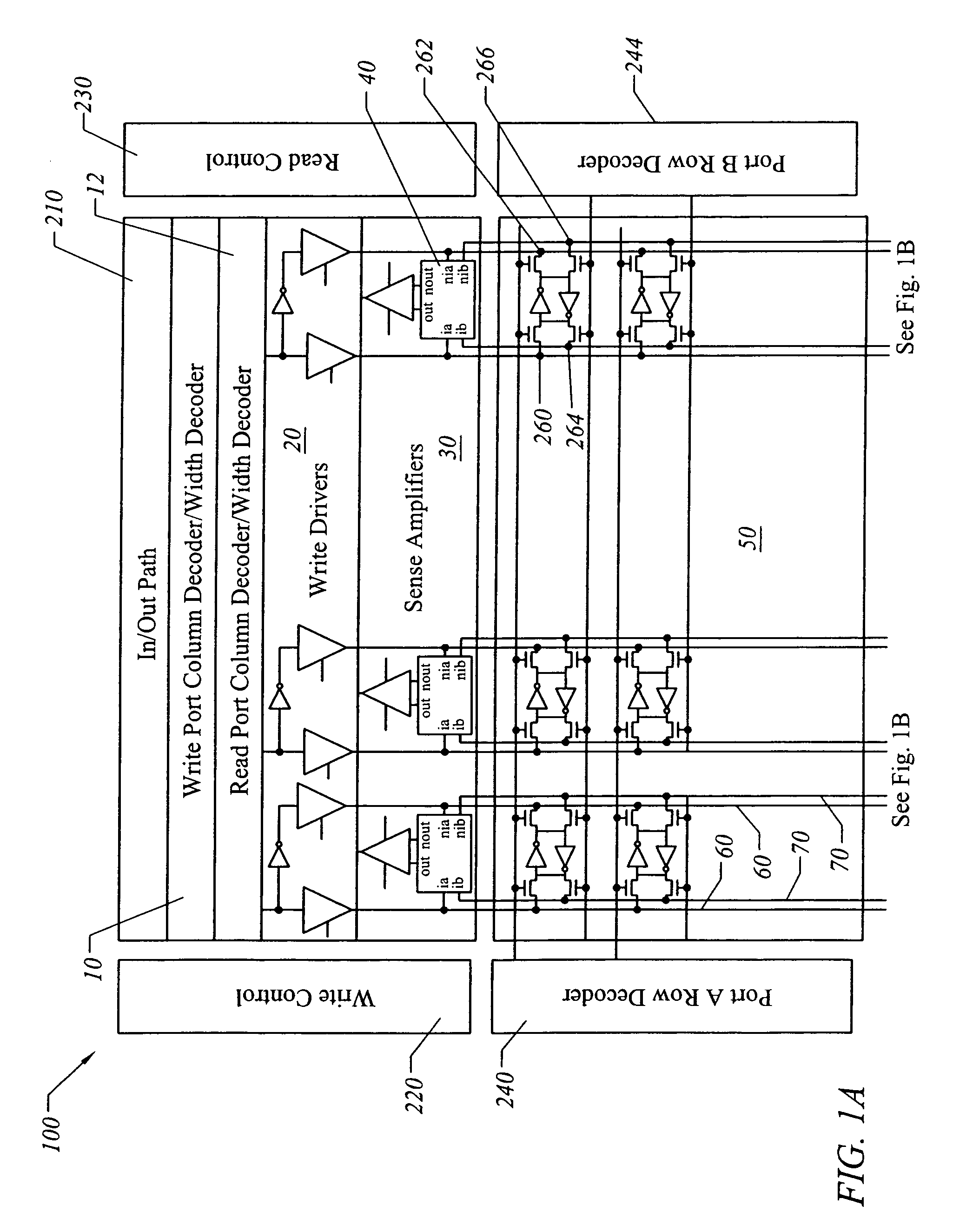
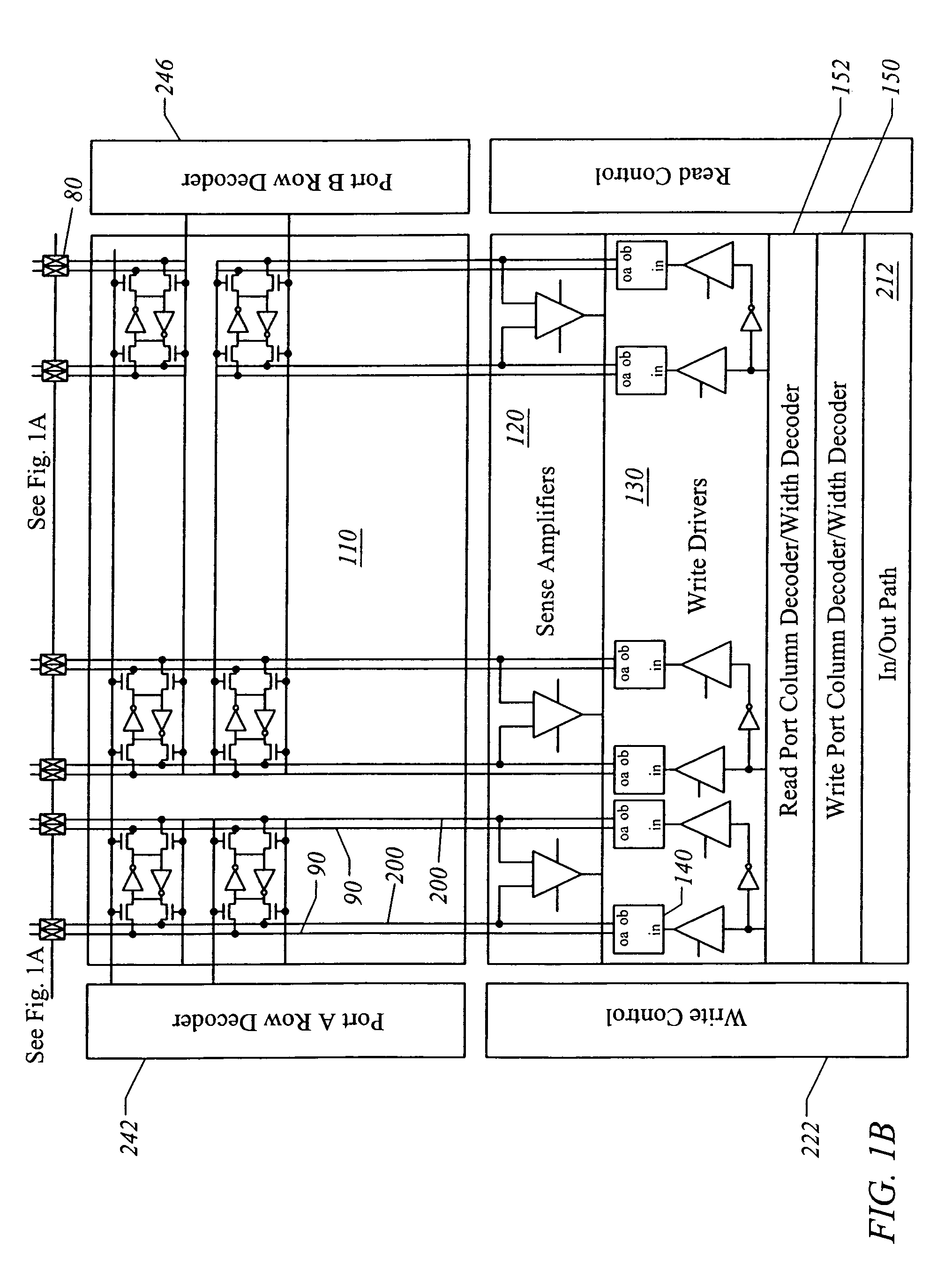
[0018]The present invention relates generally to memory systems. More specifically, the invention provides a divisible true dual port (TDP) memory system supporting simple dual port (SDP) memory subsystems. Merely by way of example, the invention has been applied to field-programmable gate arrays (FPGAs), but it would be recognized that the invention has a much broader range of applicability.

[0019]FIG. 1 is a simplified divisible memory system according to an embodiment of the present invention. This diagram is merely an example, which should not unduly limit the scope of the claims herein. The circuit 100 includes column decoders 10, 12, 150 and 152, write drivers 20 and 130, sense amplifiers 30 and 120, multiplexers 40, demultiplexers 140, memory arrays 50 and 110, bit-lines 60, 70, 90 and 200, switches 80. Additionally, the circuit 100 includes in / out paths 210 and 212, write controls 220 and 222, read controls 230 and 232, and row decoders 240, 242, 244, and 246. Although the ab...


PUM


Abstract

A random access memory circuit and a method for configuring the same. The circuit includes a first array of memory cells including a first plurality of ports and a second plurality of ports, and a second array of memory cells including a third plurality of ports and a fourth plurality of ports. Additionally, the circuit includes a plurality of switches connected to the first plurality of ports and the third plurality of ports respectively or connected to the second plurality of ports and the fourth plurality of ports respectively. Moreover, the circuit includes a plurality of sense amplifiers and a plurality of write drivers.

Description

CROSS-REFERENCES TO RELATED APPLICATIONS[0001]This application is a continuation of U.S. application Ser. No. 11 / 041,120, filed Jan. 21, 2005, now U.S. Pat. No. 7,130,238, which is incorporated by reference herein for all purposes.STATEMENT AS TO RIGHTS TO INVENTIONS MADE UNDER FEDERALLY SPONSORED RESEARCH OR DEVELOPMENT[0002]NOT APPLICABLEREFERENCE TO A “SEQUENCE LISTING,” A TABLE, OR A COMPUTER PROGRAM LISTING APPENDIX SUBMITTED ON A COMPACT DISK[0003]NOT APPLICABLEBACKGROUND OF THE INVENTION[0004]The present invention relates generally to memory systems. More specifically, the invention provides a divisible true dual port (TDP) memory system supporting simple dual port (SDP) memory subsystems. Merely by way of example, the invention has been applied to field-programmable gate arrays (FPGAs), but it would be recognized that the invention has a much broader range of applicability.[0005]An FPGA system often includes an embedded memory system. The embedded memory system can be used t...

Claims


Application Information

Patent Timeline
Patent Type & Authority Patents(United States)
IPC IPC(8): G11C8/00
CPCG11C5/025G11C7/1075G11C8/10G11C8/12H03K19/1776
Inventor YU, HAIMINGKOAY, WEI YEE
Owner ALTERA CORP
Why Eureka
Try Eureka