BMEMS-type high-sensitivity inertial sensor and manufacturing process thereof

a high-sensitivity inertial sensor and manufacturing process technology, applied in the direction of acceleration measurement using interia forces, speed measurement using gyroscopic effects, electric/magnetic means, etc., can solve the problem of reducing the capacity to reject movement in other directions, countering the improvement in sensor sensitivity, and increasing the thickness of the system

Active Publication Date: 2007-09-18
STMICROELECTRONICS SRL
View PDF12 Cites 35 Cited by
  • Summary
  • Abstract
  • Description
  • Claims
  • Application Information

AI Technical Summary

Problems solved by technology

However, the increase in the thickness determines an increase not only in the mass of the system but also in the stiffness of the springs, thus countering the improvement in the sensitivity of the sensor.
Not even other ways of increasing the mechanical sensitivity of the sensor are able to solve the problem.
For example, by making springs that are more compliant, it is possible to increase the degree of movement of the rotor for a same applied stress; however, in this case the capacity to reject movements in other directions is reduced, and the sensor could yield false readings.
However, also in this case this effect is nullified at the sensing circuit.
As for the inertial sensor 1 of FIGS. 1 and 2, then, it is not possible to increase the sensitivity of the inertial sensor simply by increasing the thickness of the structural layer.

Method used


Image

  • BMEMS-type high-sensitivity inertial sensor and manufacturing process thereof
  • BMEMS-type high-sensitivity inertial sensor and manufacturing process thereof
  • BMEMS-type high-sensitivity inertial sensor and manufacturing process thereof

Examples


Embodiment Construction

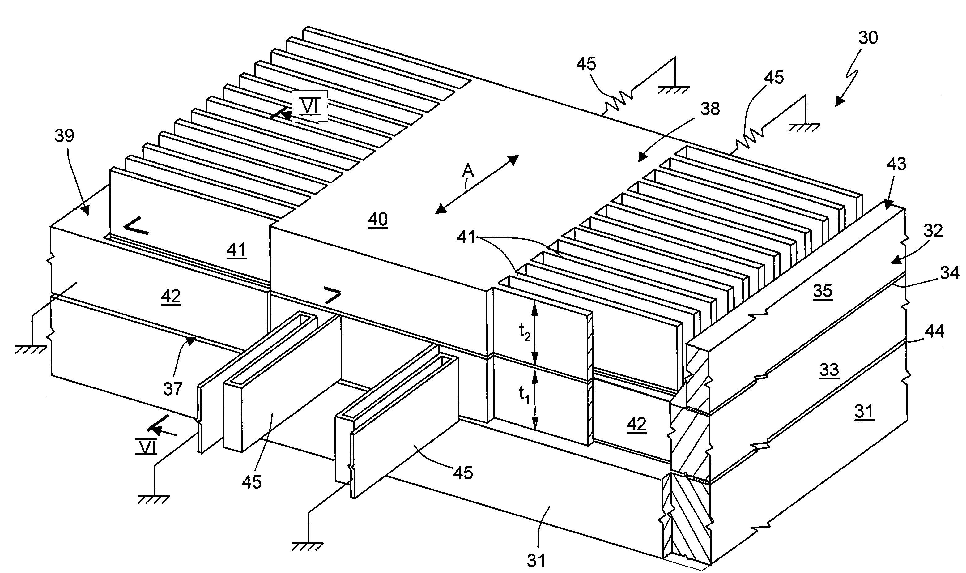
[0040]With reference to FIG. 5, an inertial sensor 30 comprises a body of semiconductor material formed by a substrate 31 and by a structural layer 32, overlying one another. In the example illustrated, the structural layer 32 is formed by a stack of layers including a bottom semiconductor layer 33, an intermediate dielectric layer 34, and a top semiconductor layer 35. As in the known inertial sensor 1, a rotor 38 and a stator 39 are formed in the structural layer 32; the rotor 38 is moreover supported by elastic elements or springs 45.

[0041]As may be noted, here the rotor 38 has a thickness greater than that of the stator 39 and of the springs 45. In fact, the rotor 38 is formed by all the layers 33-35 of the structural layer 32, while the stator 39 and the springs 45 are formed by just the bottom semiconductor layer 33, as is evident particularly from the cross-section of FIG. 6. The rotor 38, the stator 39, and the springs 45 are also here arranged at a distance from the substrat...


PUM


Abstract

The semiconductor inertial sensor is formed by a rotor element and a stator element electrostatically coupled together. The rotor element is formed by a suspended mass and by a plurality of mobile electrodes extending from the suspended mass. The stator element is formed by a plurality of fixed electrodes facing respective mobile electrodes. The suspended mass is supported by elastic suspension elements. The suspended mass has a first, larger, thickness, and the elastic suspension elements have a second thickness, smaller than the first thickness.

Description

BACKGROUND OF THE INVENTION[0001]1. Field of the Invention[0002]The present invention relates to a MEMS-type high-sensitivity inertial sensor and to the manufacturing process thereof.[0003]2. Description of the Related Art[0004]As is known, techniques of micromachining of semiconductors are used also for manufacturing electromechanical microdevices (so-called micro-electro-mechanical-systems or MEMS), such as sensors and actuators of various types. In particular, the techniques of micromachining are advantageously used for manufacturing inertial sensors, utilized for example in the automotive sector or within apparatuses equipped with stand-by functions, for recovery of functionality starting from the stand-by condition upon detection of a movement.[0005]Currently, inertial sensors are formed preferably by surface micromachining, wherein the mobile and fixed elements that form the sensor (rotor and stator and corresponding electrodes) are formed in a same structural layer, typically...

Claims


Application Information

Patent Timeline
Patent Type & Authority Patents(United States)
IPC IPC(8): G01P15/125G01C19/00G01C19/56
CPCG01C19/5755G01C19/5769
Inventor SASSOLINI, SIMONEDEL SARTO, MARCOBALDO, LORENZOMARCHI, MAURO
Owner STMICROELECTRONICS SRL
Why Eureka
Try Eureka