Inspection apparatus for pattern

A technology for inspecting devices and patterns, applied in measuring devices, electronic circuit testing, optics, etc., can solve the problems of conductive pattern damage, dust generation, etc., and achieve the effect of improving inspection accuracy

Active Publication Date: 2008-08-20
UNION ARROW TECH
View PDF1 Cites 22 Cited by
  • Summary
  • Abstract
  • Description
  • Claims
  • Application Information

AI Technical Summary

Problems solved by technology

However, most of them are structures in which the electrodes are directly in contact with the conductive pattern to provide inspection signals; in such a structure, the conductive pattern is physically contacted, which may cause damage to the conductive pattern and generation of dust, etc. question

Method used


Image

  • Inspection apparatus for pattern
  • Inspection apparatus for pattern
  • Inspection apparatus for pattern

Examples


Embodiment Construction

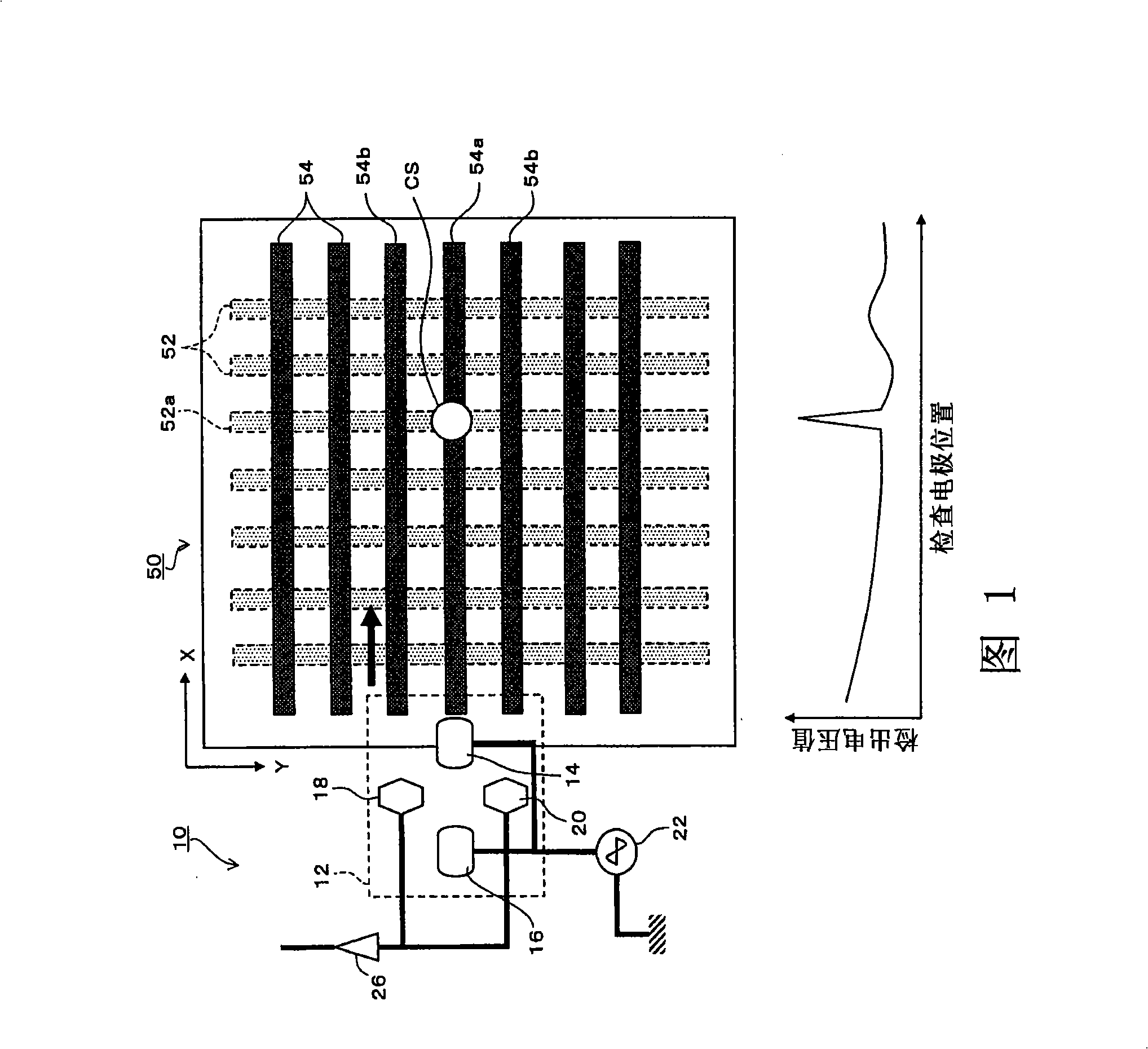
[0042] Hereinafter, embodiments of the present invention will be described with reference to the drawings. In the following description, a conductive pattern arranged in a plurality of columns on a glass substrate for use in a liquid crystal panel or the like will be inspected. However, conductive patterns used in devices other than liquid crystal panels may also be inspected as long as they are conductive patterns arranged in multiple columns.

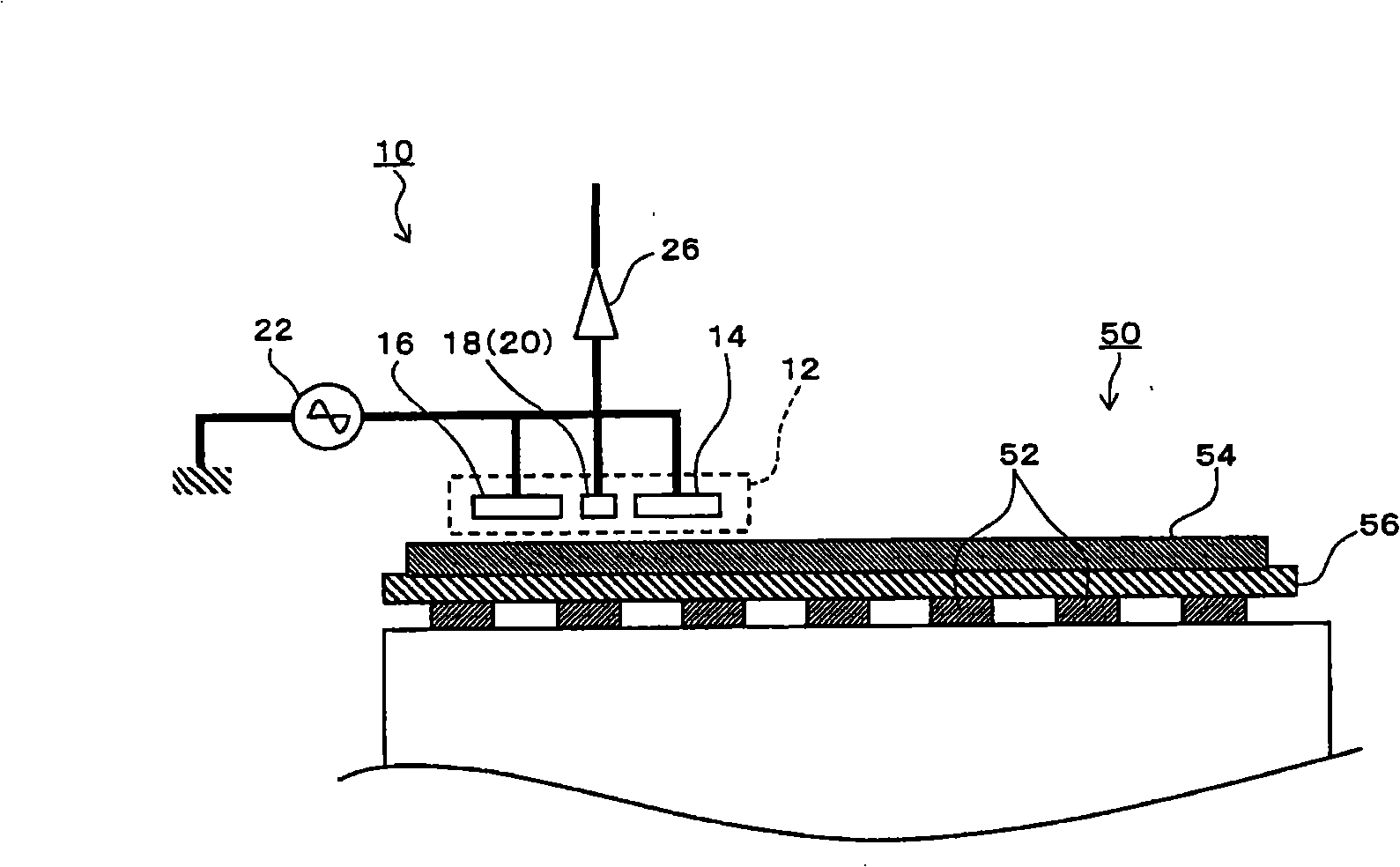
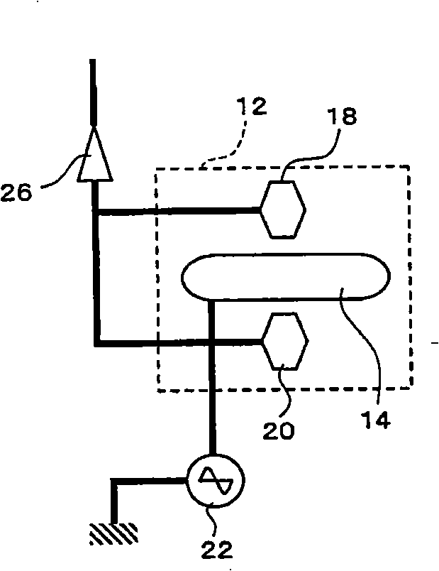
[0043] FIG. 1 is a schematic plan view of a pattern inspection device 10 according to a first embodiment of the present invention. in addition, figure 2 is its profile side view. The pattern inspection device 10 is a pattern inspection device suitable for judging the position of the cross-short circuit. Here, before describing the pattern inspection device in detail, a brief description of the cross-short circuit

[0044] A general liquid crystal panel 50 etc. is formed by stacking a first layer in which conductive patterns called...


PUM


Abstract

The invention provides a design detecting device which can judge the position of the cross short circuit without making the electrodes contact with the conductive design. Two current electrodes and two detecting electrodes are arranged on the sensor in the approximately cross shape. The sensor moves along the crossing line of the cross short circuit, wherein the current electrodes apply the AC voltage to the cross line. In addition, the detecting electrodes and the opposite grid line are in electrostatic coupling. Through the movement of the sensor, when the detecting electrodes move to the opposite position of the grid line generating the cross short circuit, the detecting electrodes respond the larger AC voltage. According to the change of the voltage value generated by induction, the position of the cross short circuit is judged.

Description

technical field [0001] The present invention relates to a pattern inspection device for inspecting conductive patterns arranged in multiple columns. Background technique [0002] In a liquid crystal panel, a first layer in which conductive patterns called gate lines and Cs lines are arranged in multiple columns and a second layer in which conductive patterns called source lines are arranged in multiple columns are superimposed. At this time, the source lines are intersected with the gate lines and the Cs lines, and an insulating layer is provided between the first layer and the second layer to prevent the source lines from being electrically connected to the gate lines and the Cs lines. However, during the manufacturing process, tiny holes, so-called pinholes, are formed in the insulating layer, so that the source line, the gate line, and the Cs line may be electrically connected (short-circuited). The short circuit of the conductive pattern between the above different laye...

Claims


Application Information

Patent Timeline
Patent Type & Authority Applications(China)
IPC IPC(8): G02F1/13G01R31/00G01R31/02
CPCG01R31/2808G02F1/1343G02F1/136286G09G3/006
Inventor 板垣卓男小原徹
Owner UNION ARROW TECH
Why Eureka
Try Eureka