

Flip-chip semiconductor package with lead frame as chip carrier and fabrication method thereof
a semiconductor and lead frame technology, applied in semiconductor devices, semiconductor/solid-state device details, electrical apparatus, etc., can solve the problems of inconvenient fabrication, inconvenient assembly, and inability to meet the requirements of the semiconductor package, so as to improve the bonding strength, increase the contact surface area, and ensure the quality of electrical connection.
- Summary
- Abstract
- Description
- Claims
- Application Information
AI Technical Summary
Benefits of technology
Problems solved by technology
Method used
Image

Examples
first preferred embodiment
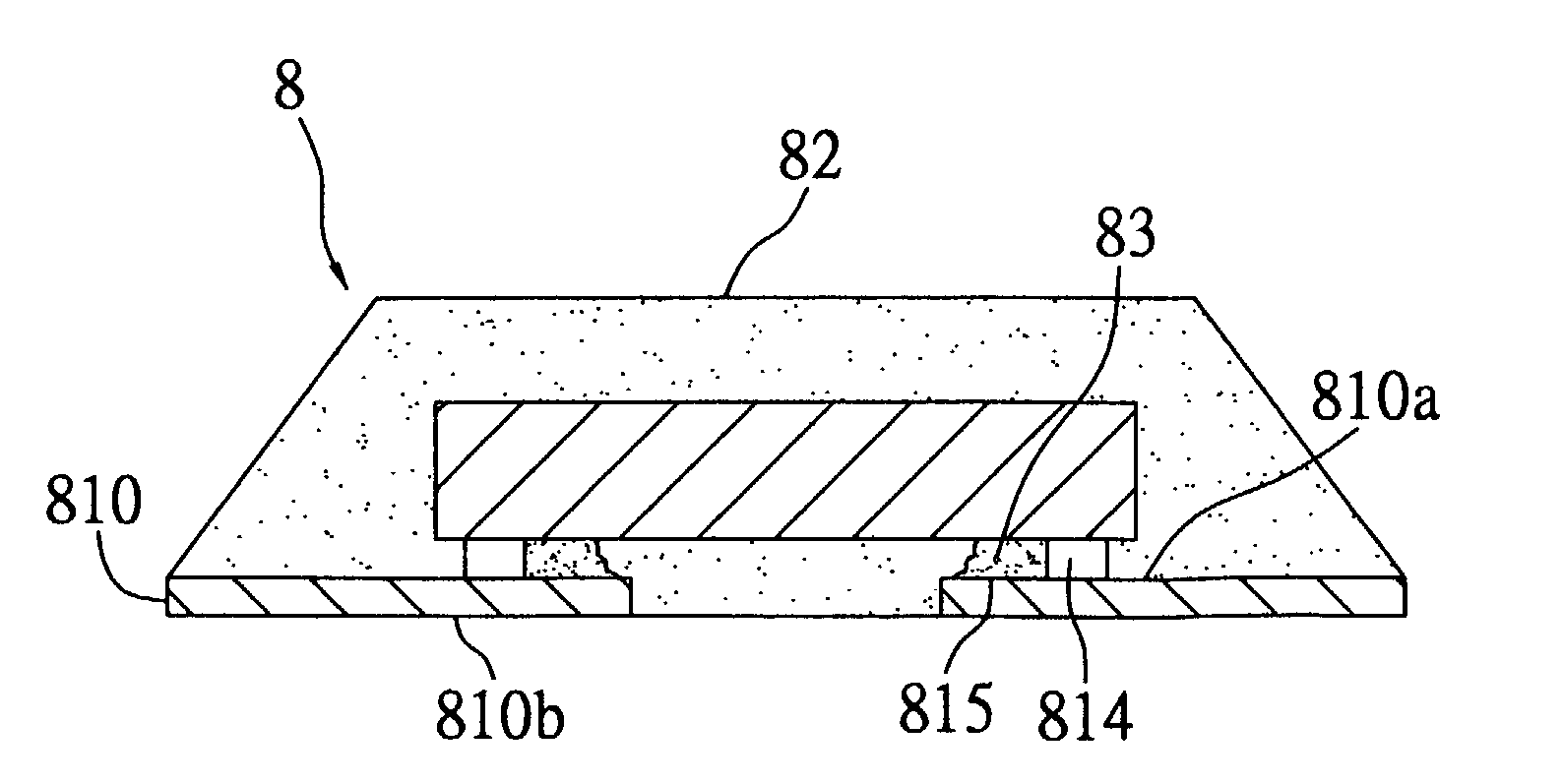
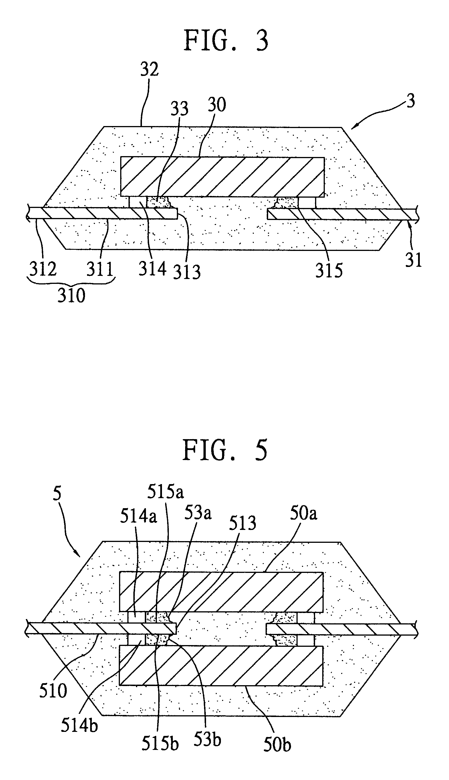
[0023]FIG. 3 illustrates a flip-chip semiconductor package with a lead frame as a chip carrier according to a first preferred embodiment of the present invention.
[0024]As shown in FIG. 3, the semiconductor package 3 is mainly composed of a chip 30, a lead frame 31 for accommodating the chip 30, and an encapsulant 32 for encapsulating the chip 30 and part of the lead frame 31.
[0025]The chip 30 is bonded with a plurality of solder bumps 33 on an active surface thereof where electronic components and electronic circuits are formed. This allows the chip 30 to be mounted on and electrically connected to the lead frame 31 by means of the solder bumps 33, so as to form a flip-chip structure.
[0026]The lead frame 31 has a plurality of leads 310, and each of the leads 310 is composed of an inner lead 311 and an outer lead 312, wherein the inner leads 311 are encapsulated by the encapsulant 32, and the outer leads 312 are exposed to outside of the encapsulant 32. The leads 310 are arranged in ...
second preferred embodiment
[0035]FIG. 5 illustrates a semiconductor package 5 according to a second preferred embodiment of the invention. As shown in FIG. 5, this semiconductor package 5 is mostly the same in structure as the semiconductor package 3 of the above first embodiment, with the only difference in that, each lead 510 in the semiconductor package 5 is provided with two polyimide tapes 514a, 514b respectively on an upper and a lower surfaces of the lead 510. This allows an upper and a lower bonding areas 515a, 515b to be respectively formed between an end 513 of the lead 510 and the polyimide tapes 514a, 514b. Thereby, an upper chip 50a can be mounted on the upper surfaces of the plurality of leads 510 by bonding solder bumps 53a formed on an upper chip 50a to the upper bonding areas 515a, and a lower chip 50b can be mounted on the lower surfaces of the leads 510 by bonding solder bumps 53b formed on a lower chip 50b to the lower bonding areas 515b, such that a multi-chip structure of the semiconduct...
third preferred embodiment
[0036]FIG. 6 illustrates a semiconductor package 6 according to a third preferred embodiment of the invention. As shown in FIG. 6, this semiconductor package 6 is mostly the same in structure as the semiconductor package 3 of the above first embodiment, with the only difference in that, at least a recessed portion 616 is formed at a bonding area 615 of a lead 610 by conventional punching or etching technique in the semiconductor package 6, so as to increase contact surface area of the bonding area 615 for bonding or wetting a solder bump 63 thereto. Thereby, for mounting the chip 60 to the plurality of leads 610, solder bumps 63 implanted on a chip 60 would be more firmly reflow-soldered and wetted to the bonding areas 615 with the recessed portions 616, and thus bonding strength between the solder bumps 63 and the leads 610 can be effectively enhanced.
[0037]The recessed portion 616 can be shaped in cross-section as, but not limited to, a rectangular, arc or conical recess. The rece...
PUM
 Abstract
Description
Claims
Application Information