Multi-layer printed circuit board fabrication system and method

Inactive Publication Date: 2007-10-16
ORBOTECH LTD
View PDF34 Cites 18 Cited by
  • Summary
  • Abstract
  • Description
  • Claims
  • Application Information

AI Technical Summary

Benefits of technology

[0043]wherein fewer than 50% of the elements of the alignment pattern in the image overlay the pattern in the identical pattern for any position in which the patterns are not aligned.

Problems solved by technology

Among the problems which arise in printed circuit board fabrication is the side to side alignment of printed circuit patterns on various substrate layers, and mutual alignment among patterns printed on various substrate layers.

Method used


Image

  • Multi-layer printed circuit board fabrication system and method
  • Multi-layer printed circuit board fabrication system and method
  • Multi-layer printed circuit board fabrication system and method

Examples


Embodiment Construction

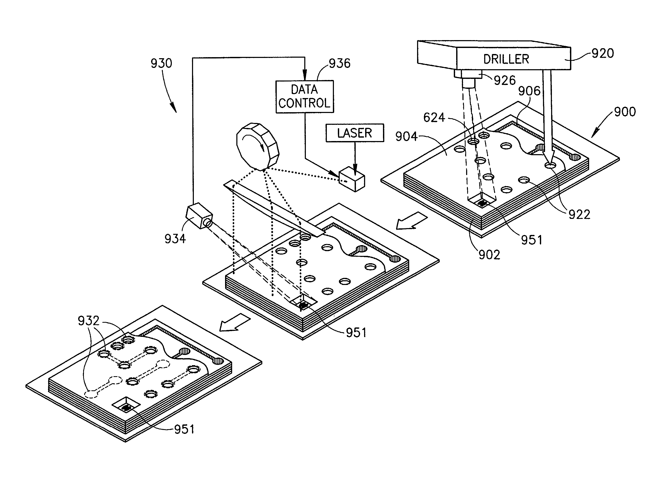
[0074]FIGS. 3 and 4 show an embodiment 200 of the present invention, which includes apparatus enabling the use of a new method of determining the relative position of the printed circuit board in the scanner useful for aligning images to be written on the respective opposing sides of a printed circuit board.

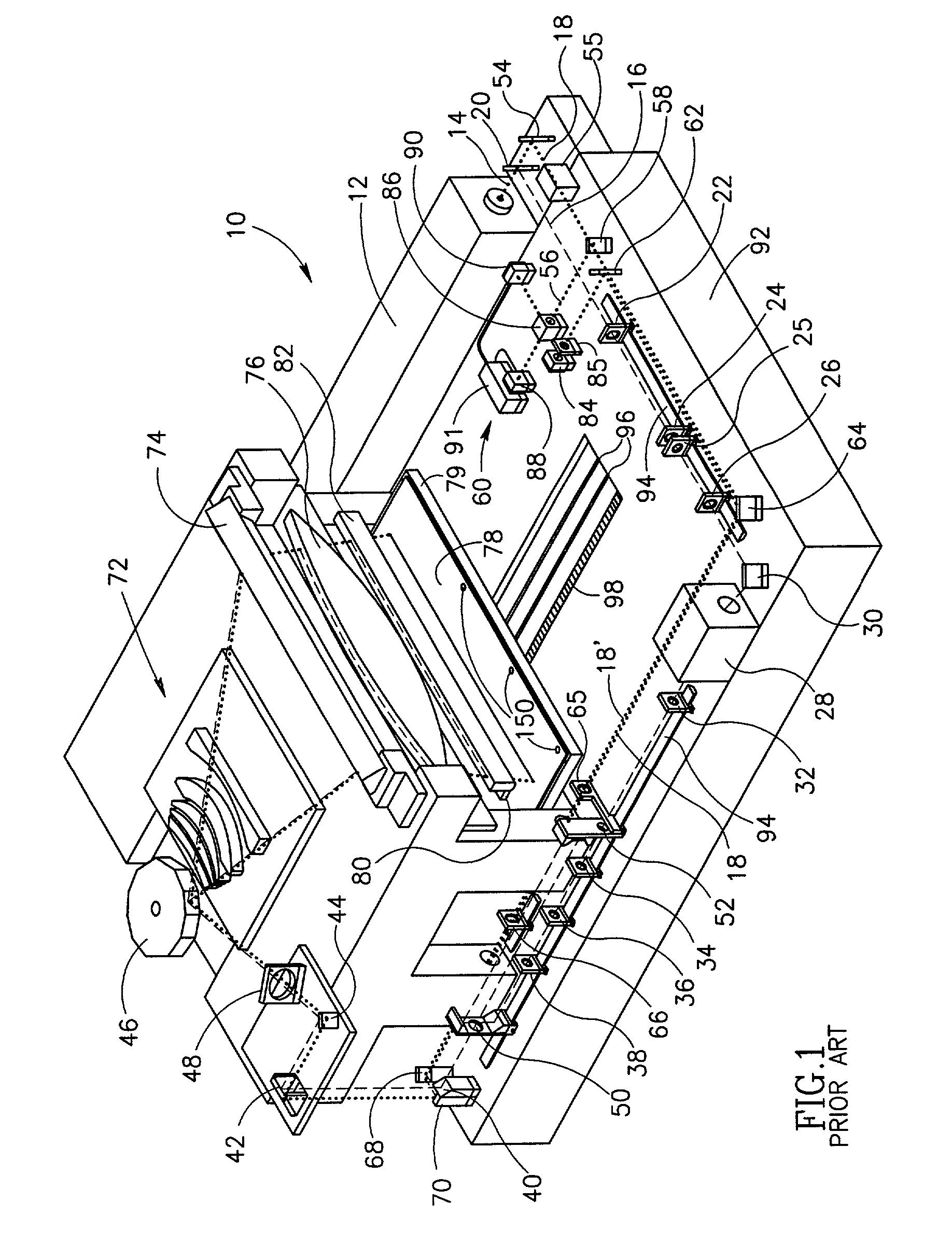
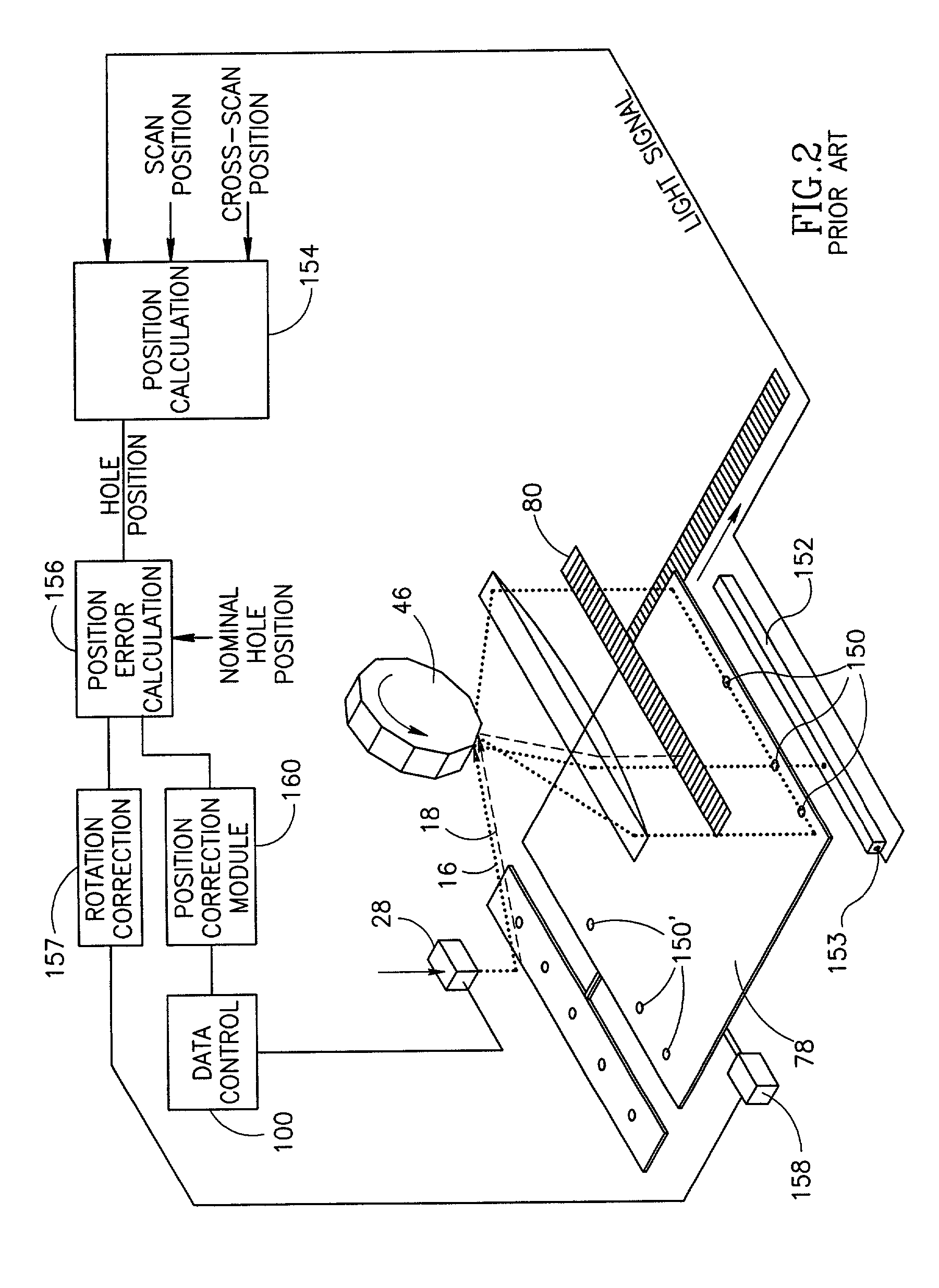
[0075]In this system, a principal difference from the prior art system of FIGS. 1 and 2 resides in the mechanism for determining a reference for the scanner for writing an electrical circuit pattern.

Scanner—Imager Coordinate Calibration

[0076]It is appreciated that in order to align patterns that are sequentially recorded on a substrate a mechanism is required to coordinate between the respective location of the subsequently recorded patterns. In exemplary embodiments of the invention, an acquired image of a reference pattern is employed. It is desirable to tie together the location of the reference pattern in images to coordinate space of the scanner system to ensure that recorde...


PUM

PropertyMeasurementUnit
laser direct imagingaaaaaaaaaa
transparentaaaaaaaaaa
electricalaaaaaaaaaa

Abstract

A method for aligning an image to be recorded by a direct image scanner on an upper layer of a printed circuit board with an image recorded on a lower layer thereof, the method comprising:
    • visually imaging a portion of the image on the lower layer; and
    • recording a pattern on the upper layer, referenced to coordinates of the visual image of the portion.

Description

RELATED APPLICATIONS[0001]This application is a continuation-in-part of U.S. patent application Ser. No. 09 / 708,160, filed Nov. 8, 2000 now U.S. Pat. No. 6,701,197 and is a continuation-in-part of U.S. patent application Ser. No. 09 / 792,498, filed Feb. 23, 2001 now U.S. Pat. No. 6,819,789.FIELD OF THE INVENTION[0002]The present invention is related to the field of electrical circuit fabrication and especially to the field of printed circuit board fabrication employing a laser direct imaging device.BACKGROUND OF THE INVENTION[0003]It is known to manufacture printed circuit boards by way of a so-called sequentially build up methodology in which at least one outer layer is sequentially added to an already existing printed circuit board core.[0004]Systems for recording electrical circuit patterns on printed circuit board substrates include exposure systems employing projectors and phototool type mask having an image of an electrical circuit formed onto a transparent film.[0005]PCT paten...

Claims


Application Information

Patent Timeline
Patent Type & Authority Patents(United States)
IPC IPC(8): G06K9/00G03F7/20G03F9/00G06T1/00G06T3/20H04N1/113H05K1/02H05K3/00H05K3/46
CPCG03F7/2053G03F9/00H05K1/0269H05K3/4679H05K3/0008H05K2201/09918H05K3/0082H05K3/4652H05K2201/09063H05K3/0035
Inventor GANOT, AMNONGINO, HANANHANINA, GOLANKANTOR, ZEEVKLING, BORISSPINZI, SHABTAYBEN-EZRA, BARRY
Owner ORBOTECH LTD
Why Eureka
Try Eureka