Optical coupling to IC chip

a technology of optical coupling and ic chip, which is applied in the field of coupling of optical signals, to achieve the effects of high volume optical coupling, low cost, and variance in optical coupling of the subassembly

Inactive Publication Date: 2007-11-20
APPLIED MATERIALS INC
View PDF14 Cites 130 Cited by
  • Summary
  • Abstract
  • Description
  • Claims
  • Application Information

AI Technical Summary

Benefits of technology

[0010]The optical coupling configurations described herein includes optical elements that are both external to the IC structure and integral to the IC structure. They provide optical coupling from the light source or optical fiber to the IC waveguide. Likewise, the same optical coupling configurations provide optical coupling from an IC waveguide to an external waveguide or optical waveguide of a different IC. The optical coupling configuration, which includes a fiber pigtailed collimating lens mount structure subassembly, also referred to as a “Surface Mount Optical Coupler” or “SMOC”, can be fabricated so that it is very low cost, is scaleable for high volume optical coupling to IC manufacturing, and is compatible with the optical design for coupling to IC waveguides that have the IC coupling optics described in this disclosure.
[0011]Some of the concepts described herein enable one to design the optical coupling alignment and attachment processing to be compatible with electronics industry automated assembly processing equipment of surface mount assembly using Flip-Chip automated assembly equipment. Also certain embodiments of the SMOC make it possible that many variances in optical coupling of the subassemblies can be greatly compensated solely by lateral displacement of the SMOC relative to the IC backside lens. This compensation requires that the beam not be perfectly collimated at the output of the SMOC so that other errors in beam tilt and position at image locations of the fiber and waveguide can be compensated by lateral movement of the SMOC. The less collimated the beam, the less movement is required by the SMOC to compensate for lateral tilt and position errors in other elements of the optical system. So a careful analysis needs to be made to determine the best non-collimation or beam divergence / convergence that fits the desired tolerances on the system. In that case, the SMOC design and assembly processing methods ensure that no tilt of the SMOC relative to the IC optics can occur to degrade the optical coupling. These advances, which are described herein, when combined together enable a low-cost, high volume production solution for optical coupling to ICs.
[0012]Using two lenses with one on the coupler and the other on the IC allows for larger placement tolerance between the collimated, or pseudo-collimated, light beams in between the “focusing lens” into the IC waveguide and the “collimating lens” from the optical fiber due to larger beam diameter. Optical coupling alignment tolerances on the order of 20 μm for 400 μm beam diameters and 5 μm for 100 μm beams can be expected. In addition, integrating the focusing lens into the IC by wafer level fabrication reduces the Bill of Materials (BOM) and assembly align & attach costs of this lens.
[0013]Choosing a small diameter for the collimated beam allows for both a shorter optical train length and smaller footprint area on the IC backside heat sink. This is also beneficial from an optics perspective due to the closer proximity of the focusing lens to the IC waveguide (partly due to IC wafer thinning factors), resulting in a smaller than normal (400-800 μm for traditional optoelectronic devices) collimated beam diameter.
[0014]At least some of the embodiments disclosed herein provide a means for optically coupling to optical waveguides within integrated chips that has low cost fabrication of components and has assemblies that are compatible with high volume production assembly. The theoretical optical coupling efficiency is 96% for some of these systems. Various disclosed design features allow for this high optical coupling efficiency to be realized in a production environment.

Problems solved by technology

Getting the optical signals into and out of the IC chips in a way that is commercially practical and involves fabrication costs that are competitive presents one of the challenges the industry faces today.

Method used


Image

  • Optical coupling to IC chip
  • Optical coupling to IC chip
  • Optical coupling to IC chip

Examples


Embodiment Construction

Structure:

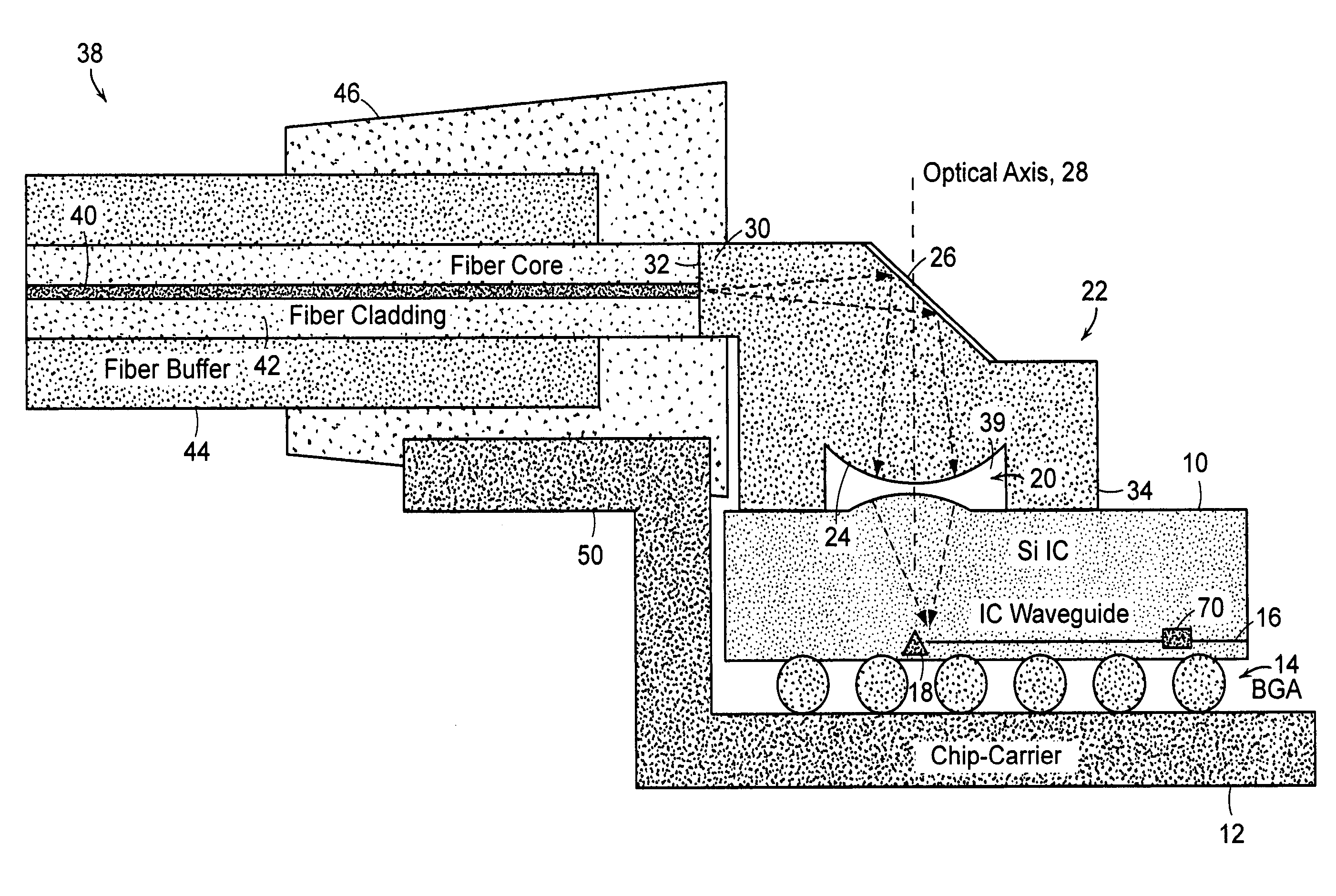
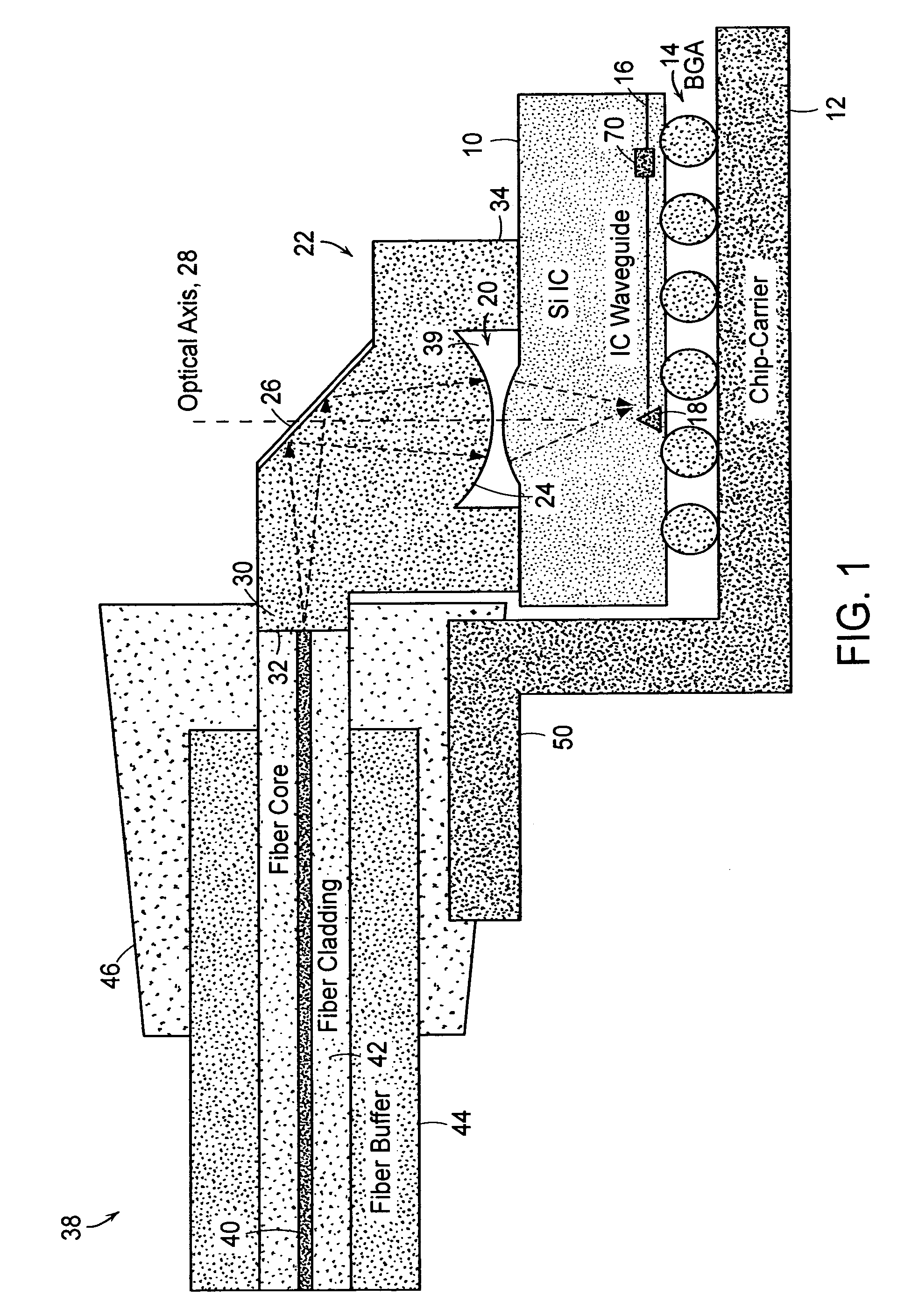
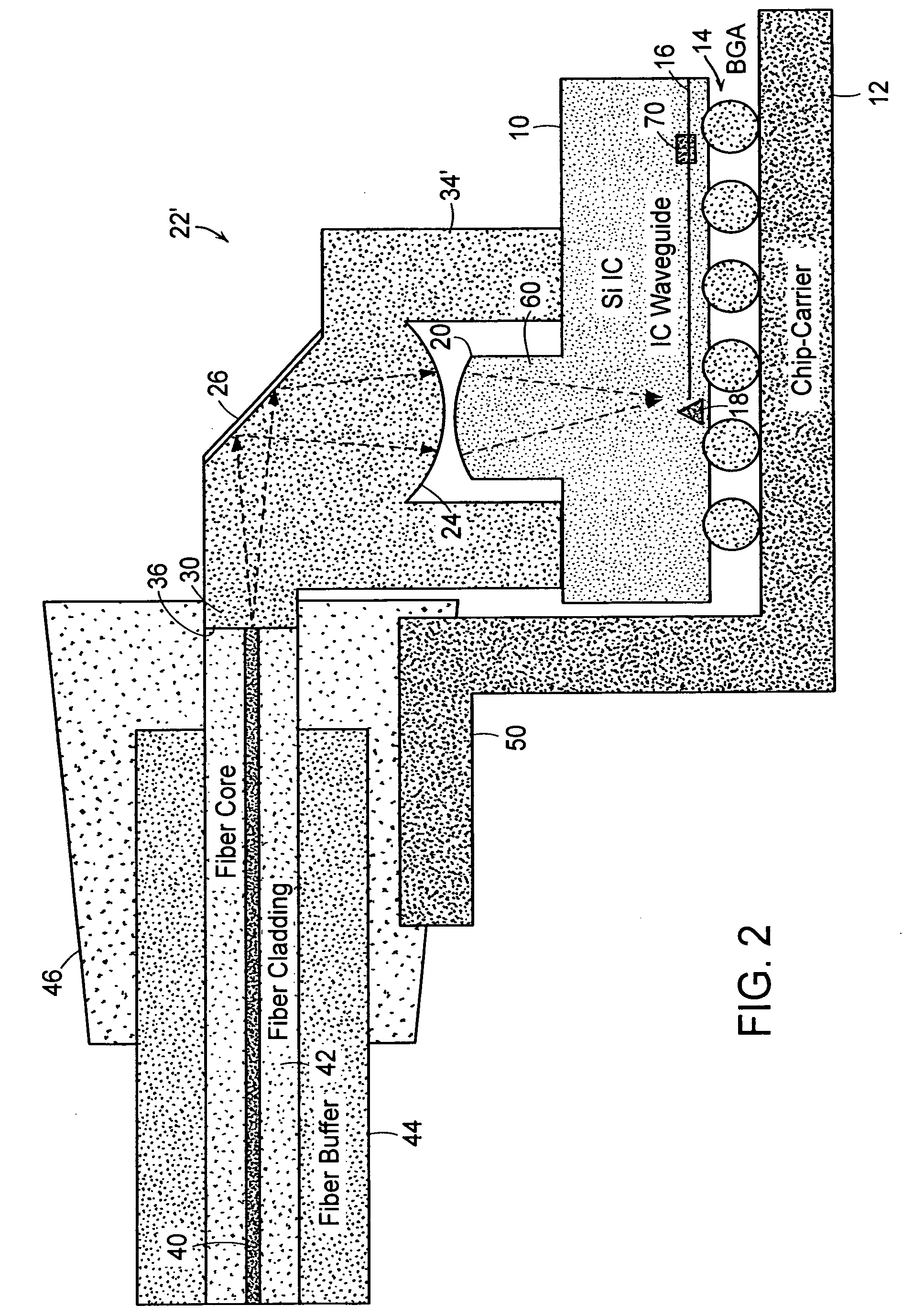
[0035]Embodiments are described herein that represent various structures for coupling optical signals to optical waveguides that have been fabricated on or in an IC chip. In general, in these embodiments the optical coupling to the IC waveguide is accomplished by directing a beam (which may be a diverging beam, a converging beam or a collimated beam) to a Si lens fabricated on and integral to the backside of the IC chip (i.e., silicon substrate). In at least some of the described embodiments, the beam will be a substantially collimated beam. The Si lens then focuses the light beam into the IC waveguide via a 45° mirror located at the IC waveguide. The collimated light beam between the external optics and the IC optics passes through dry air. The collimating lens and the Si focusing lens both have anti-reflection (AR) coatings to keep the optical coupling losses low.

[0036]One embodiment is illustrated in FIG. 1. It shows an IC chip 10 that is flip-chip mounted onto a chip c...


PUM

PropertyMeasurementUnit
angleaaaaaaaaaa
diametersaaaaaaaaaa
diametersaaaaaaaaaa

Abstract

An optoelectronic circuit including: an IC chip made up of a substrate in which an optical waveguide and a mirror have been fabricated, the substrate having a first lens formed thereon, wherein the mirror is aligned with the optical waveguide and the first lens is aligned with the mirror to form an optical path connecting the first lens, the mirror, and the optical waveguide; and an optical coupler including a second lens, the optical coupler affixed to the substrate and positioned to align the second lens with the first lens so as to couple an optical signal into or out of the optical waveguide within the IC chip.

Description

This application also claims the benefit of U.S. Provisional Application No. 60 / 653,432, filed Feb. 16, 2005, incorporated herein by reference.TECHNICAL FIELD[0001]This invention relates generally to the coupling of optical signals into and out of an IC chip.BACKGROUND OF THE INVENTION[0002]Semiconductor fabrication technology is moving towards figuring out ways to combine both electrical signaling and optical signaling on the same IC chips. This drive to combine of the two technologies is in part fueled by the inherent advantages associated with optical signals in comparison to electrical signals both in terms of distributing information throughout a given IC chip and in terms of inter-chip communications. One application that is likely to be among early commercial implementations involves the use of optical signals to distribute clock signals throughout a very large IC chip, such as a microprocessor. This is because optical signals are typically characterized by smaller skews and ...

Claims


Application Information

Patent Timeline
Patent Type & Authority Patents(United States)
IPC IPC(8): G02B6/32B29B11/00
CPCG02B6/4206G02B6/423G02B6/4214G02B6/4204G02B6/4249G02B6/30G02B6/32G02B6/42
Inventor PALEN, EDWARD L.WOJCIK, GREGORY L.WEST, LAWRENCE C.
Owner APPLIED MATERIALS INC
Why Eureka
Try Eureka