Contact and electrical connecting apparatus

a technology of electrical connection and electrical connection device, which is applied in the direction of coupling device connection, measurement instrument housing, instruments, etc., can solve the problems of defective semiconductor devices, electrical connecting devices cannot conduct kelvin inspection of semiconductor devices,

Active Publication Date: 2007-12-04
NIHON MICRONICS
View PDF9 Cites 12 Cited by
  • Summary
  • Abstract
  • Description
  • Claims
  • Application Information

AI Technical Summary

Benefits of technology

[0027]According to the present invention, the first and second base portions are made to confront each other in their thickness direction with the electrical insulator interposed. The first terminal contact portion extends toward the second base portion without coming into electrical contact with the second contact piece, and the second terminal contact portion extends toward the first base portion without coming into electrical contact with the first contact piece. Further, the first and second terminal contact portions extend in the thickness direction of the first and second base portions, i.e., in a direction orthogonal to the extending direction of the terminal of the semiconductor device.
[0028]Since this enables the first and second terminal contact portions to come electrically in contact with the terminal of the semiconductor device over a wide range, the Kelvin connection between the contacts and the terminal can be surely made.
[0029]Also, electrical contact between the first contact piece and the second base portion can be surely prevented by forming, in the electrical insulator of the contact, the first contact preventing portion for preventing electrical contact between the first terminal contact portion and the second base portion as well as for preventing electrical contact between the second terminal contact portion and the first base portion, and the second contact preventing portion projecting into a gap formed between the first and second terminal contact portions and for preventing electrical contact between the first terminal contact portion and the second terminal contact portion.
[0030]The terminal can be electrically connected to the first and second terminal contact portions by giving them in their thickness direction a thickness dimension greater than the total thickness dimension of the first and second body portions and the electrical insulator and the same as or less than the total thickness dimension of the first body portion, the electrical insulator and the second body portion.
[0031]Also, by forming a space between the first conductive contact portion and the second conductive contact portion, a space is formed between the electrical insulator and one and the other of the conductive portions. This makes it hard for the electrical insulator enter between the first conductive contact portion and one of the conductive portions as well as between the second conductive contact portion and the other of the conductive portions, thereby ensuring a Kelvin connection between the contact and the terminal.
[0032]The electrical insulator includes a pair of electrical insulating sheet confronting each other, and by disposing an adhesive between the pair of electrical insulating sheets, both electrical insulating sheets are relatively movable in parallel. Due to this, when the contact is pressed against the terminal and the pair of conductive portions in a state of being inclined to the terminal and the pair of conductive portions, both contact pieces relatively move against the adhesive strength of the adhesive. This makes the first and second conductive contact portions to surely come into contact with the terminal and the conductive portion, respectively.

Problems solved by technology

Accordingly, since the electrical connecting apparatus and the semiconductor device cannot constitute a Kelvin connection, the electrical connecting apparatus cannot conduct a Kelvin inspection of the semiconductor device.
Such a semiconductor device is judged as a defective product even if electrical characteristics are good.

Method used


Image

  • Contact and electrical connecting apparatus
  • Contact and electrical connecting apparatus
  • Contact and electrical connecting apparatus

Examples


Embodiment Construction

Contact

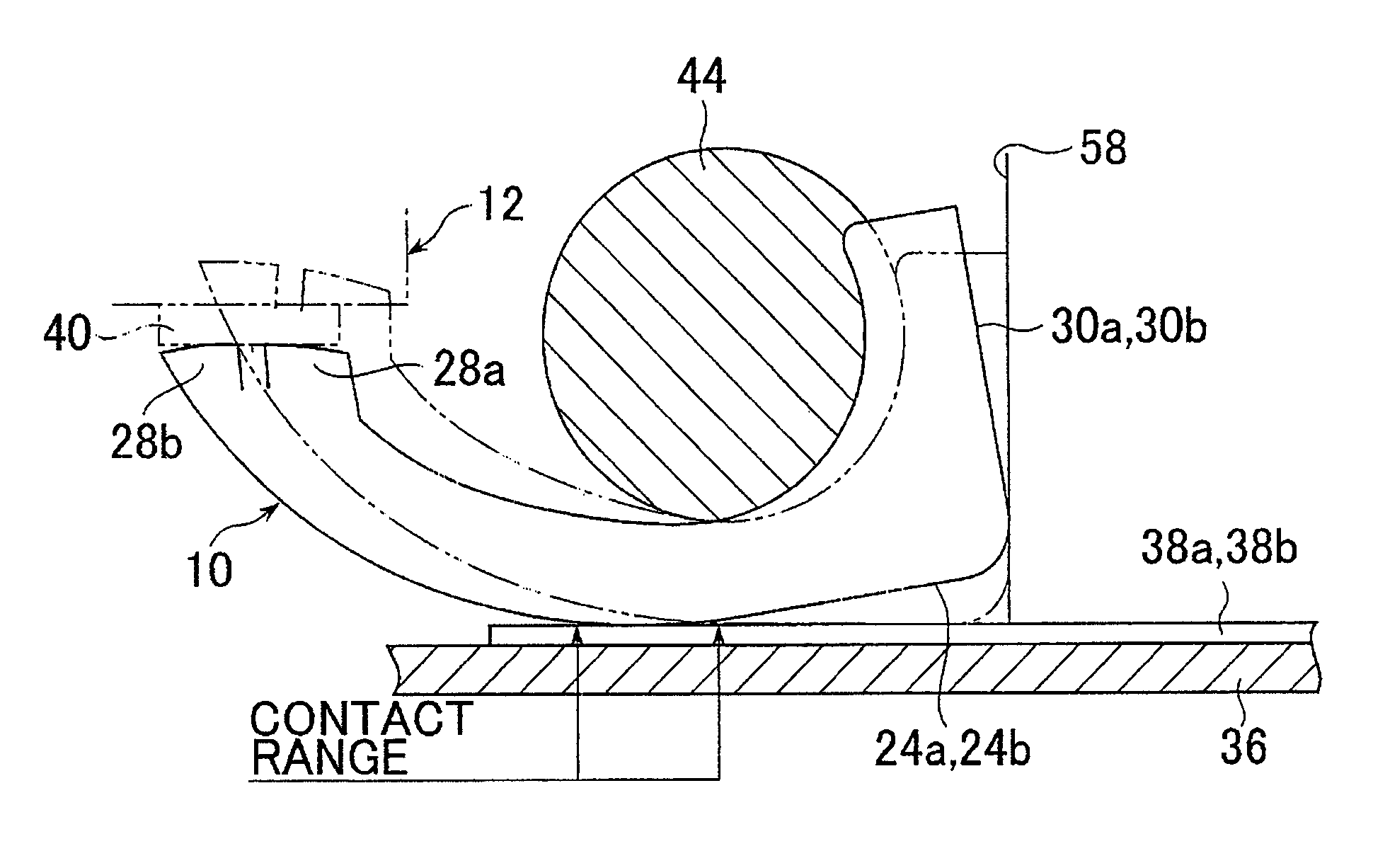
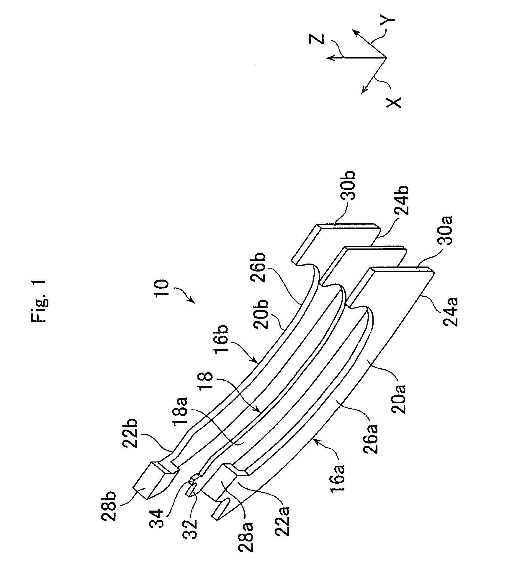
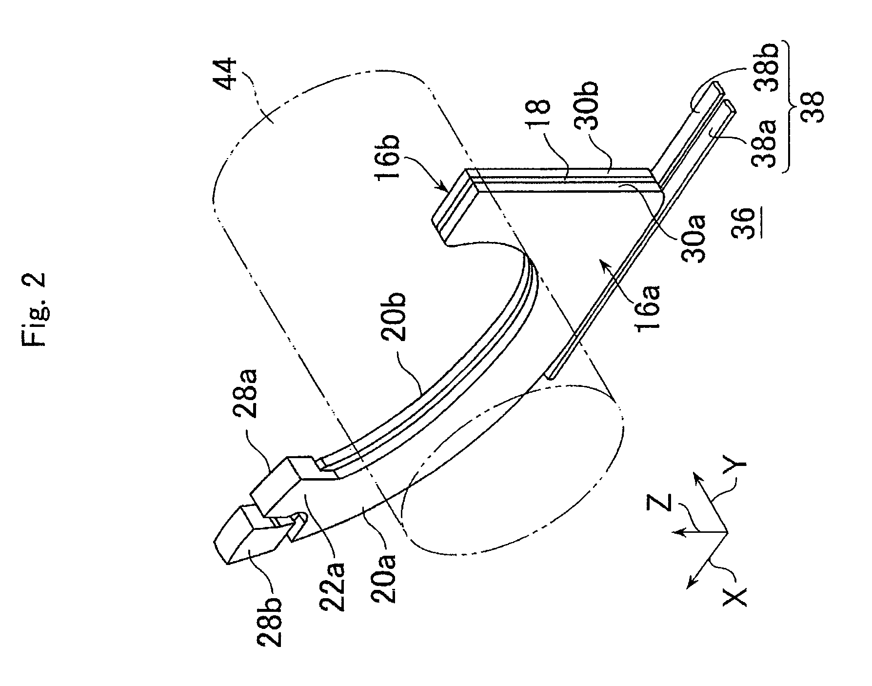
[0067]Referring to FIGS. 1 through 4, a contact 10 is used as a probe of an electrical connecting apparatus 14 (see FIG. 7) in an inspection or a test of a semiconductor device 12 (see FIG. 7) such as an integrated circuit.

[0068]The contact 10 includes a first and a second conductive contact pieces 16a and 16b and at least one sheet-like electrical insulator 18 such as polyimide.

[0069]The first contact piece 16a is provided with a plate-like first body portion 26a and a first terminal contact portion 28a. The first body portion 26a has a base portion 20a, a first elongate portion 22a extending from the first base portion 20a, a first conductive contact portion 24a formed in the first base portion 20a. The first terminal contact portion 28a is formed in the first elongate portion 22a.

[0070]The second contact piece 16b is provided with a plate-like second body portion 26b and a second terminal contact portion 28b. The second body portion 26b has a base portion 20b, a second el...


PUM


Abstract

A contact includes: a first and a second conductive contact pieces and at least one sheet-like electrical insulator such as polyimide. Each contact piece has a sheet-like body portion having a base portion, an elongate portion extending from the base portion, and a conductive contact portion formed in the base portion; and a terminal contact portion formed in the elongate portion. Both base potions are made to confront each other in their thickness direction with an electrical insulator interposed, such that one of the terminal contact portions, without being in electrical contact with the second contact piece, extends toward the second base portion, while the other terminal contact portion, without being in electrical contact with the first contact piece, extends toward the first base portion.

Description

CROSS REFERENCE TO RELATED APPLICATIONS[0001]This application claims the priority benefit of copending PCT / JP2004 / 008072, filed Jun. 3, 2004 which is incorporated herein by reference.TECHNICAL FIELD[0002]The present invention relates to a contact and an electrical connecting apparatus to be used for electric test of a semiconductor device such as an integrated circuit.BACKGROUND OF THE INVENTION[0003]An inspection or a test of electric characteristics of a packaged or molded semiconductor device, in particular, an integrated circuit (IC), is generally conducted by utilizing an inspection socket, i.e., a test socket for removably mounting a semiconductor device as an auxiliary unit for inspection.[0004]In one of electrical connecting apparatus of this type, a plurality of probes, i.e., contacts bent substantially in J-shape are used (Japanese Patent Appln. Public Disclosure (KOKAI) No. 2003-123874).[0005]In this prior art, each contact comprises a base portion bent substantially in J...

Claims


Application Information

Patent Timeline
Patent Type & Authority Patents(United States)
IPC IPC(8): H01R12/00G01R1/04G01R1/067H01R33/76
CPCG01R1/0466H01R12/714G01R1/06733
Inventor OSATO, EICHIGOTO, YOSHIHITO
Owner NIHON MICRONICS
Why Eureka
Try Eureka