

Contact and electrical connecting apparatus
- Summary
- Abstract
- Description
- Claims
- Application Information
AI Technical Summary
Benefits of technology
Problems solved by technology
Method used
Image

Examples
Embodiment Construction
Contact
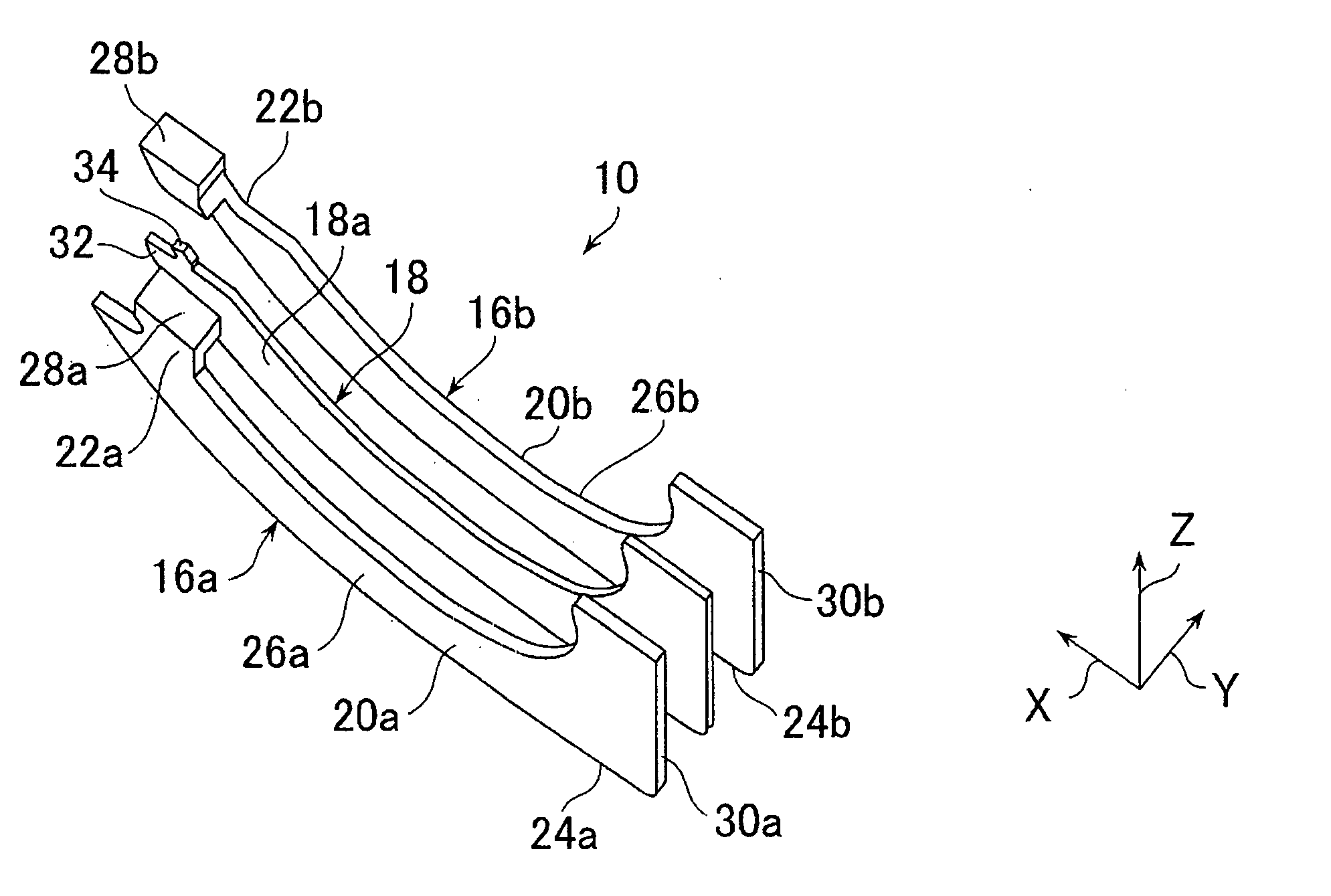
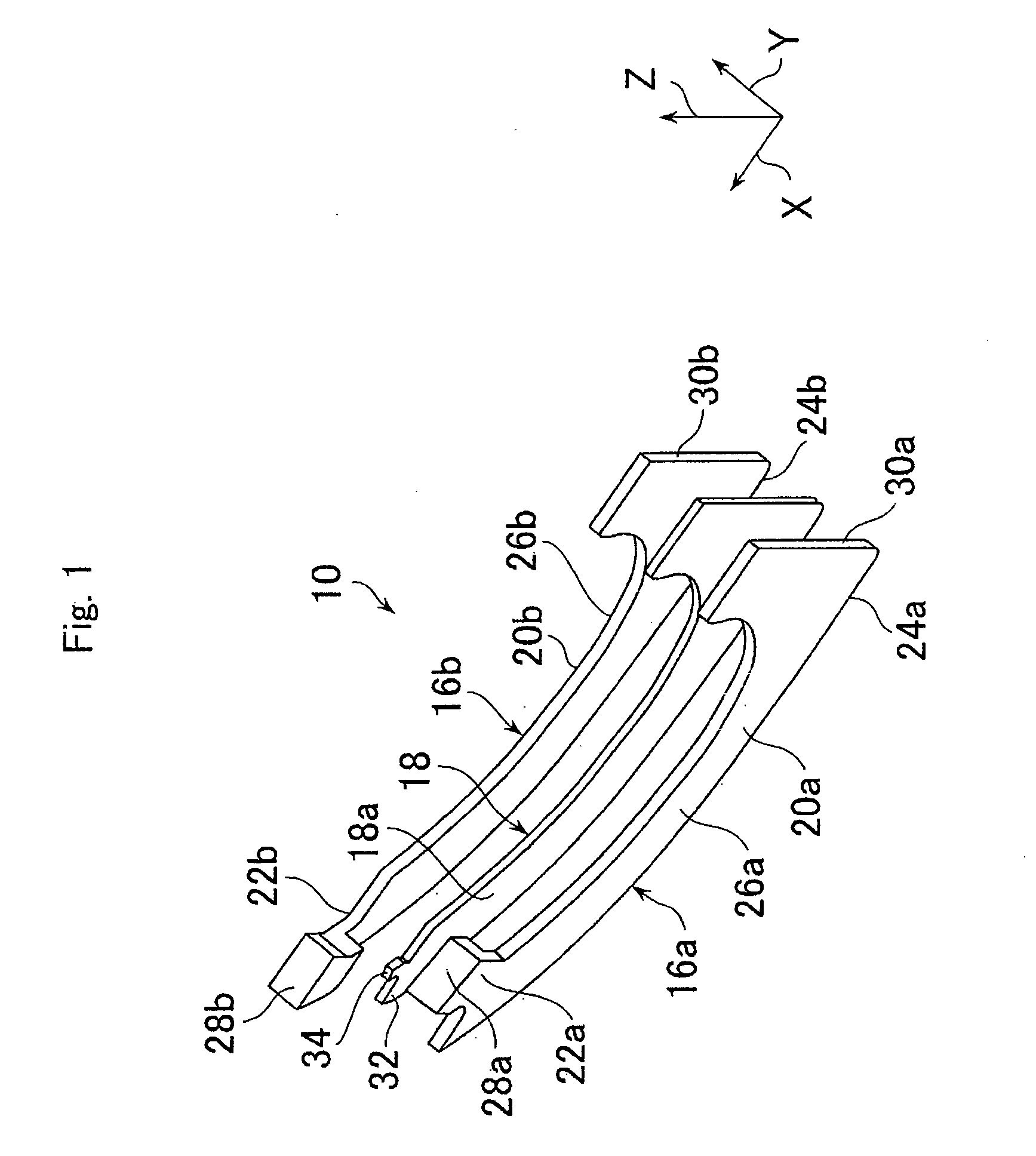
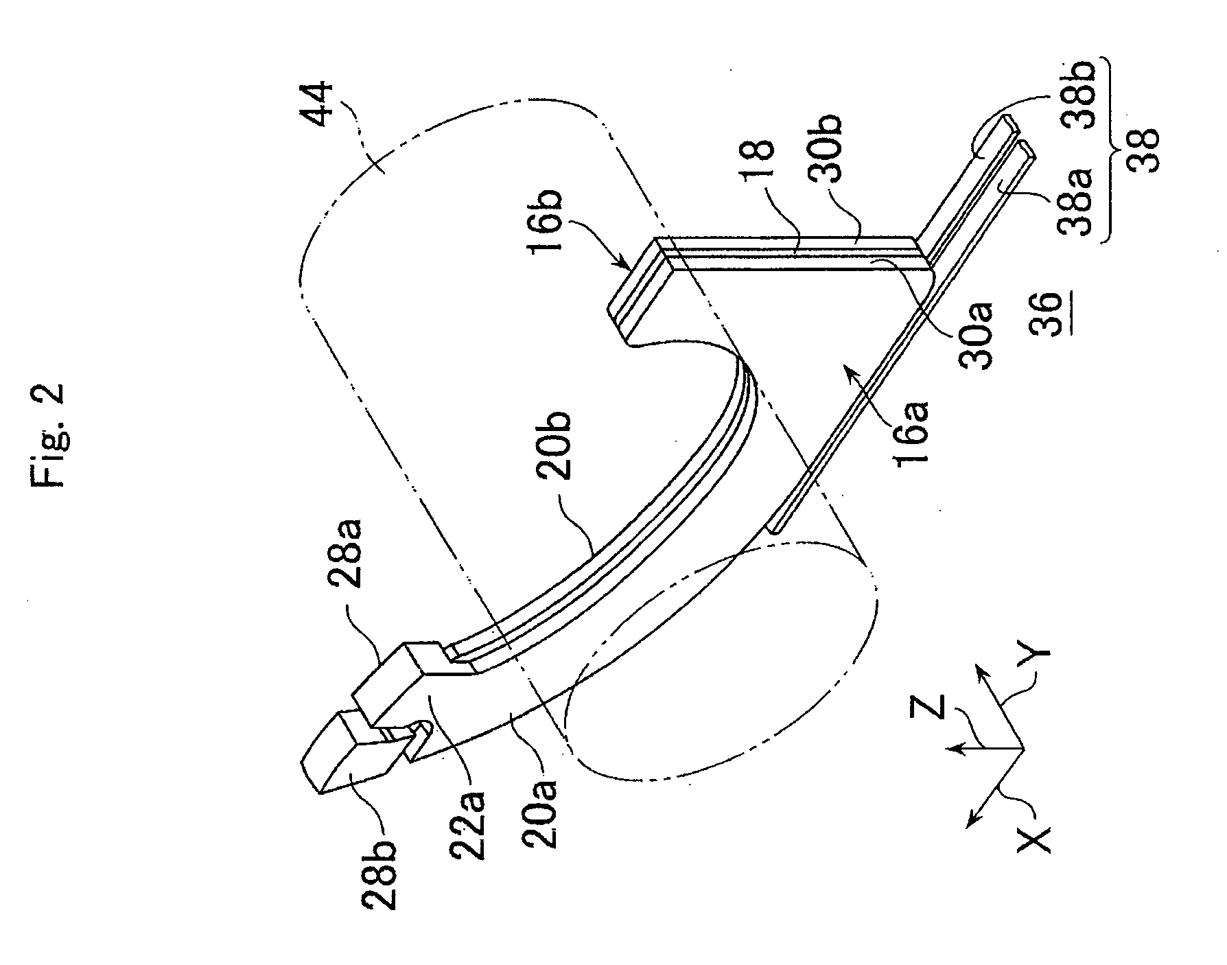
[0067] Referring to FIGS. 1 through 4, a contact 10 is used as a probe of an electrical connecting apparatus 14 (see FIG. 7) in an inspection or a test of a semiconductor device 12 (see FIG. 7) such as an integrated circuit.
[0068] The contact 10 includes a first and a second conductive contact pieces 16a and 16b and at least one sheet-like electrical insulator 18 such as polyimide.
[0069] The first contact piece 16a is provided with a plate-like first body portion 26a and a first terminal contact portion 28a. The first body portion 26a has a base portion 20a, a first elongate portion 22a extending from the first base portion 20a, a first conductive contact portion 24a formed in the first base portion 20a. The first terminal contact portion 28a is formed in the first elongate portion 22a.
[0070] The second contact piece 16b is provided with a plate-like second body portion 26b and a second terminal contact portion 28b. The second body portion 26b has a base portion 20b, a s...
PUM
 Abstract
Description
Claims
Application Information