Apparatus and method for picking up semiconductor chip

Active Publication Date: 2007-12-11
PANASONIC CORP
View PDF17 Cites 25 Cited by
  • Summary
  • Abstract
  • Description
  • Claims
  • Application Information

AI Technical Summary

Benefits of technology

[0004]In such a circumstance, the present invention intends to provide an apparatus for picking up a semiconductor chip whic

Problems solved by technology

However, such a low-profiled semiconductor device is apt to be damaged and so difficult to handle.
Particularly, it is very difficult to execute a process of taking out an individual semiconductor chip cut from a wafer.
In this case, if the method for separating a semiconductor chip, which has been conventionally used, is adopted for the low-profiled semiconductor chip (see Patent Publication JP-A-54-58356), i.e. pushing up the semiconductor chip by a needle

Method used


Image

  • Apparatus and method for picking up semiconductor chip
  • Apparatus and method for picking up semiconductor chip
  • Apparatus and method for picking up semiconductor chip

Examples


Embodiment Construction

[0019]Now referring to the drawings, an explanation will be given of an embodiment of the present invention.

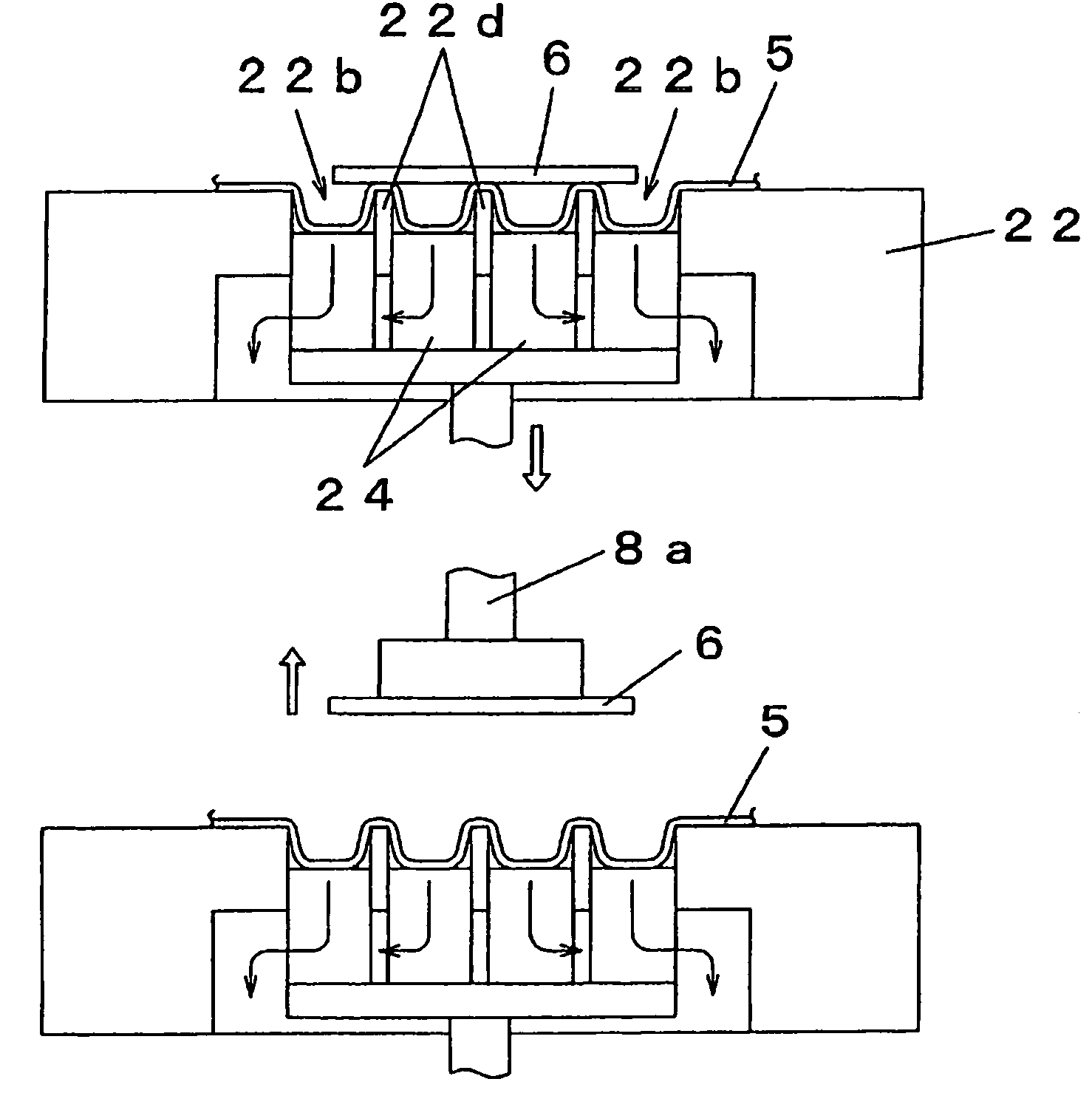
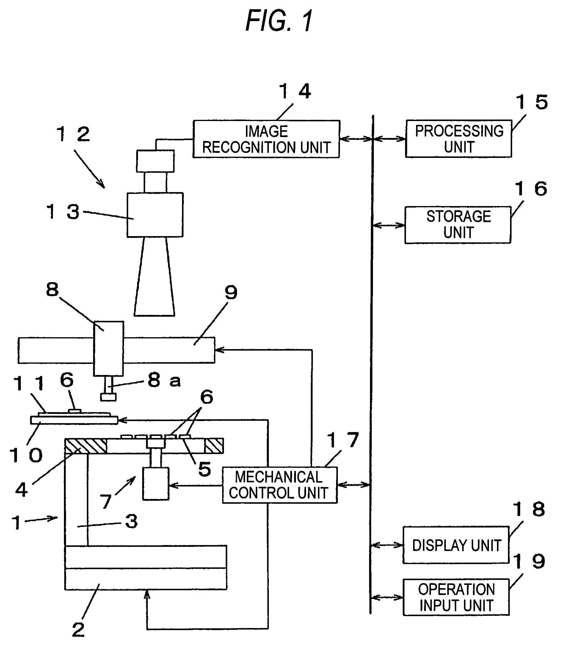
[0020]First, referring to FIG. 1, an explanation will be given of the configuration of a semiconductor chip used in the present invention. In FIG. 1, a chip supplying portion, generally 1 is designed in a structure in which a holding table 4 is connected onto a bracket 3 upstanding on an XY table 2. On the holding table 4, a sheet 5 is held on which a large number of semiconductor chips 6 (hereinafter simply referred to as chips 6) are adhered.

[0021]Now, the chip 6 is a low-profiled chip having a characteristic of small rigidity and flexibility. The sheet 5 is made of flexible silicone resin. The sheet 5, on which the chip 6 are adhered, is apt to easily warp together with the chip 6. In the separating operation described later, using this property of the sheet 5, the sheet 5 as well as the chips is warped so that the sheet 5 is separated from the lower surface of the chip 6.

[...


PUM


Abstract

A semiconductor chip pick-up apparatus includes: a pick-up head for picking up the chip on a sheet; a holding table for holding the sheet; a recognition means for recognizing the chip; a positioning means for positioning the chip relatively to the pick-up head on the basis of the recognition result by the recognition means; and a sheet separating mechanism for separating the sheet from the chip by sucking the sheet from a suction plane brought in contact with a lower surface of the sheet. The sheet separating mechanism includes: a plurality of sucking grooves formed in the suction plane; a plurality of boundary zones, each of which separates the sucking grooves adjacent to each other and supports the sheet in their contact with the lower surface of the sheet during sucking; suction members movably arranged in the sucking grooves, respectively so that when they are moved toward lower surface of the sheet, they are brought into contact with the lower surface of the sheet to suck the sheet; a moving means for moving the suction members; and a sucking means for sucking the sheet from said plurality of sucking grooves.

Description

BACKGROUND OF THE INVENTION[0001]The present invention relates to an apparatus for picking up a semiconductor chip adhered on a sheet cut from a wafer and a method for picking up the same.[0002]A semiconductor chip has a tendency of being low-profiled with recent downsizing of electronic components, and a very low-profiled semiconductor device having a thickness of 100 μm or less has been put into practice. However, such a low-profiled semiconductor device is apt to be damaged and so difficult to handle. Particularly, it is very difficult to execute a process of taking out an individual semiconductor chip cut from a wafer. This process repeatedly implements the operation of picking up the semiconductor chip adhered on a sheet using an suction nozzle while being separated for each piece. In this case, if the method for separating a semiconductor chip, which has been conventionally used, is adopted for the low-profiled semiconductor chip (see Patent Publication JP-A-54-58356), i.e. pu...

Claims


Application Information

Patent Timeline
IPC IPC(8): B32B38/10H01L21/46H01L21/00H01L21/68H01L21/683
CPCH01L21/67132H01L21/681H01L21/6838Y10S438/976Y10T156/1983Y10T156/1105Y10T156/1978Y10T156/1944Y10T156/1179Y10T156/1906
Inventor KASAI, TERUAKI
Owner PANASONIC CORP
Why Eureka
Try Eureka