

Touch panel, and input device and electronic apparatus each equipped with the touch panel
- Summary
- Abstract
- Description
- Claims
- Application Information
AI Technical Summary
Benefits of technology
Problems solved by technology
Method used
Image

Examples
first embodiment
(First Embodiment)
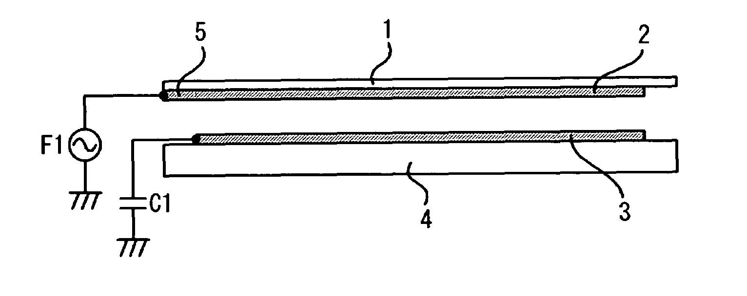
[0035]First, a first embodiment of the present invention will be described in detail. FIGS. 3A and 3B illustrate the structure of a touch panel 10 in accordance with this embodiment. FIG. 3A is a top view of the touch panel 10, and FIG. 3B is a section view of the touch panel 10, taken along the line A-A′of FIG. 3A.
[0036]As shown in FIGS. 3A and 3B, the touch panel 10 includes two films 1 and 4 that are arranged to face each other, with a spacer (not shown) forming a predetermined gap G between the films 1 and 4. The touch panel 10 also includes transparent electrodes 2 and 3 formed on the facing surfaces of the films 1 and 4, respectively In this embodiment, the facing surfaces having the transparent electrodes 2 and 3 formed thereon are flat surfaces of the same square shape.
[0037]As shown in FIG. 3B, one of the transparent electrodes 2 and 3 (the transparent electrode 2 on the upper layer in the example shown in FIG. 3B) has a stub (a power supply unit) 5 that i...
second embodiment
(Second Embodiment)
[0047]Referring now to FIGS. 6A and 6B, a second embodiment of the present invention will be described in detail. FIGS. 6A and 6B illustrate the structure of a touch panel 20 in accordance with this embodiment. FIG. 6A is a top view of the touch panel 20, and FIG. 6B is a section view of the touch panel 20, taken along the line A-A′of FIG. 6A.
[0048]As shown in FIGS. 6A and 6B, the touch panel 20 includes two films 1 and 4 that are arranged to face each other, with a spacer (not shown) forming a predetermined gap G between the films 1 and 4. The touch panel 20 also includes transparent electrodes 22 and 23 formed on the facing surfaces of the films 1 and 4, respectively. In this embodiment, the touch panel 20 further includes a transparent electrode 26 formed on the opposite surface of the film 4 to the surface on which the transparent electrode 23 is formed.
[0049]The transparent electrode 26 covers the entire back surface of the film 4, and is grounded via a capac...
third embodiment
(Third Embodiment)
[0058]Referring now to FIGS. 7A through 7D, a third embodiment of the present invention will be described in detail. FIGS. 7A through 7D illustrate the structure of a touch panel 30 in accordance with this embodiment. FIG. 7A is a top view of an upper layer 30u and a lower layer 30d included in the touch panel 30. FIG. 7B is a partial view of the back surface of the upper layer 30u. FIG. 7C is a top view of the upper layer 30u arranged over the lower layer 30d. FIG. 7D is a section view of the touch panel 30, taken along the line A-A′of FIG. 7C.
[0059]As shown in FIGS. 7A through 7D, a strip-line transparent electrode 32 having electrode fingers 32a arranged in parallel with one another is patterned on the upper layer 30u of the touch panel 30. In this structure, a power supply unit 32b is provided at one end of the common wire of the electrode fingers 32a. A radiofrequency is inputted to or outputted from the transparent electrode 32 through the power supply unit 3...
PUM
 Abstract
Description
Claims
Application Information