Article having electromagnetic coupling module attached thereto

a technology of electromagnetic coupling and electromagnetic coupling, which is applied in the structure of radiating elements, resonant antennas, instruments, etc., can solve the problems of difficult to attach wireless antennas to a variety of articles, difficult to reduce feed circuit size, and negligible so as to increase the frequency range of transmission signals, reduce feed circuit size, and reduce the effect of negative effect of other elements

Active Publication Date: 2011-12-20
MURATA MFG CO LTD
View PDF265 Cites 7 Cited by
  • Summary
  • Abstract
  • Description
  • Claims
  • Application Information

AI Technical Summary

Benefits of technology

[0010]In the article having an electromagnetic coupling module attached thereto according to a preferred embodiment of the present invention, the antenna gain is determined by the size of the dielectric body. Accordingly, even when the size of the electromagnetic coupling module is reduced, a sufficient gain can be obtained. In addition, the frequency of a transmission signal radiated from the dielectric body and the frequency of a reception signal supplied to the wireless IC chip are substantially the same as a self-resonance frequency of the feed circuit of the feed circuit board. Accordingly, accurate positioning of the electromagnetic coupling module bonded onto the dielectric body is not required, and therefore, the electromagnetic coupling module can be easily bonded onto the dielectric body. Furthermore, a maximum gain of the transmission and reception signals is substantially determined by at least one of the size and shape of the feed circuit board, a distance between the feed circuit board and the dielectric body, and a medium disposed between the feed circuit board and the dielectric body.
[0012]In addition, the article having an electromagnetic coupling module attached thereto can preferably further include an impedance conversion interconnection electrode disposed in close proximity to the electromagnetic coupling module. The impedance conversion interconnection electrode may be disposed on or inside the dielectric body. Alternatively, the impedance conversion interconnection electrode may be provided on another dielectric body, and the other dielectric body is disposed on or inside the dielectric body. By providing the impedance conversion interconnection electrode, the transmission efficiency of the electromagnetic waves can be improved.
[0014]In the article having an electromagnetic coupling module attached thereto according to a preferred embodiment of the present invention, it is preferable that the feed circuit is a lumped constant resonant circuit including a capacitance element and an inductance element. The lumped constant resonant circuit may preferably be one of an LC series resonant circuit and an LC parallel resonant circuit. Alternatively, the lumped constant resonant circuit may be configured so as to include a plurality of LC series resonant circuits or a plurality of LC parallel resonant circuits. The resonant circuit may be defined by a distributed constant resonant circuit. In such a case, an inductor of the resonant circuit is preferably defined by a stripline. However, if the resonant circuit is defined by a lumped constant resonant circuit that includes a capacitance element and an inductance element, the size of the feed circuit can be easily reduced and have a negligible negative effect of the other elements, such as the radiator. If the resonant circuit includes a plurality of resonant circuits, the frequency range of the transmission signal can be increased by coupling the plurality of resonant circuits with one another.
[0015]In addition, by arranging the capacitance element between the wireless IC chip and the inductance element, surge resistance can be improved. Since surge is a low-frequency electrical current having a frequency of about 200 MHz or less, the surge can be reduced by using a capacitor. Therefore, the wireless IC chip can be protected from surge damage.
[0016]The feed circuit board can preferably be a multilayer board formed by stacking a plurality of dielectric layers or a plurality of magnetic layers. In such a case, the capacitance element and the inductance element are disposed on a surface of the multilayer board and / or inside the multilayer board. By forming the resonant circuit using a multilayer board, components (e.g., interconnection electrodes) of the resonant circuit can preferably be disposed inside the board as well as on the board. Accordingly, the size of the board can be reduced. In addition, the layout of the components of the resonant circuit can be freely designed, and therefore, the performance of the resonant circuit can be easily improved. The multilayer board may preferably be a resin multilayer board formed by stacking a plurality of resin layers or may be a ceramic multilayer board formed by stacking a plurality of ceramic layers. Alternatively, the multilayer board may preferably be a thin-film multilayer board formed by using a thin-film forming technology. When the multilayer board is a ceramic multilayer board, it is preferable that the ceramic layers are made of a low-temperature co-fired ceramic material. This is because silver and copper having a low resistance value can preferably be used for resonant circuit members.
[0018]The feed circuit board may be a rigid or flexible board made of a resin or a ceramic, for example. If the board is rigid, the frequency of a transmission signal can be stabilized even when a wireless IC device is bonded to a dielectric body having any shape. In addition, the wireless IC chip can be stably mounted on the rigid board.

Problems solved by technology

However, since the size of the wireless IC device is relatively large, the wireless IC device cannot be attached to a small article.
Accordingly, the attachment procedure is relatively complicated.
Therefore, it is difficult to attach the wireless antenna to a variety of articles even when it is desired that the wireless antenna be used in various ways.

Method used


Image

  • Article having electromagnetic coupling module attached thereto
  • Article having electromagnetic coupling module attached thereto
  • Article having electromagnetic coupling module attached thereto

Examples


twelfth example

of Electromagnetic Coupling Module

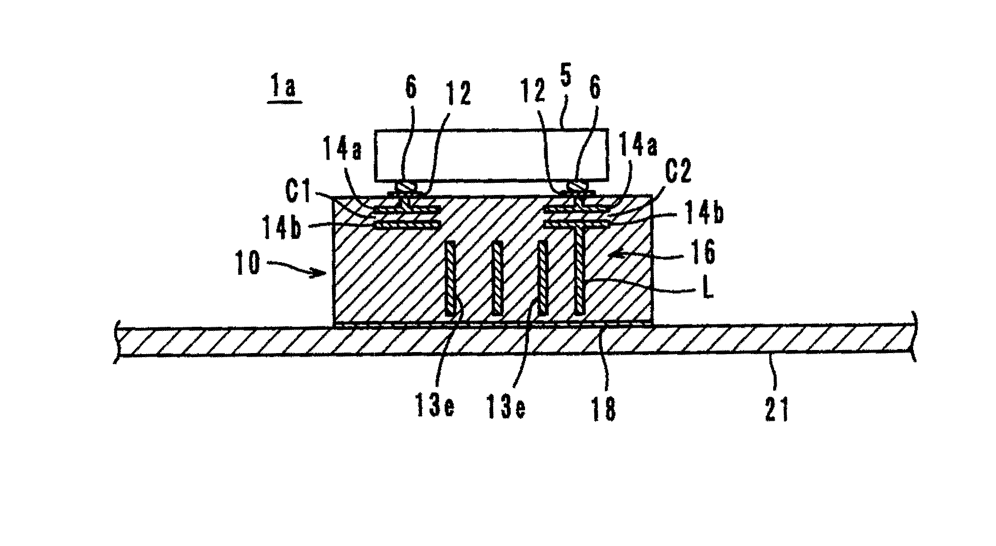
[0130]As shown by an equivalent circuit in FIG. 35, in an electromagnetic coupling module 1l, which is a twelfth example, a feed circuit 16 includes inductance elements L1 and L2 that are coupled to each other via a magnetic field. One end of the inductance element L1 is connected to a wireless IC chip via the capacitance element C1, while the other end is connected to ground. The inductance element L2 is connected to the one end of the inductance element L1 via the capacitance element C2, while the other end is connected to ground. That is, the feed circuit 16 includes an LC series resonant circuit including the inductance element L1 and the capacitance element C1 and an LC series resonant circuit including the inductance element L2 and the capacitance element C2. The resonant circuits are coupled with each other using magnetic field coupling indicated by the mutual inductance M. In addition, each of the inductance elements L1 and L2 is coupled to ...


PUM


Abstract

An article having an electromagnetic coupling module attached thereto includes an electromagnetic coupling module and a PET bottle having the electromagnetic coupling module bonded thereto. The electromagnetic coupling module includes a wireless IC chip arranged to process transmission and reception signals and the feed circuit board having the wireless IC chip mounted thereon. The feed circuit board includes a feed circuit including a resonant circuit having a predetermined resonant frequency. The feed circuit performs characteristic impedance matching between the PET bottle and the wireless IC chip. The PET bottle functions as a radiator arranged to radiate a transmission signal supplied from the feed circuit using electromagnetic field coupling and to supply a received reception signal to the feed circuit using electromagnetic field coupling.

Description

BACKGROUND OF THE INVENTION[0001]1. Field of the Invention[0002]The present invention relates to an article having an electromagnetic coupling module attached thereto and, in particular, to an article having an electromagnetic coupling module including a wireless IC chip attached thereto that is used for a radio frequency identification (RFID) system.[0003]2. Description of the Related Art[0004]Recently, RFID systems have been developed. In RFID systems, a reader / writer that generates an induction field communicates with an IC tag (hereinafter, referred to as a wireless IC device) attached to an article in a non-contact manner. Thus, information is communicated therebetween. Examples of the wireless IC device used in the RFID system include a wireless IC device described in Japanese Unexamined Patent Application Publication No. 2006-203187.[0005]The wireless IC device described in Japanese Unexamined Patent Application Publication No. 2006-203187 includes an antenna made of a metal ...

Claims


Application Information

Patent Timeline
Patent Type & Authority Patents(United States)
IPC IPC(8): H01Q1/38
CPCG06K7/10178H04B5/0012G06K19/07749G06K19/04H01L2224/16225
Inventor KATO, NOBORUDOKAI, YUYAIKEMOTO, NOBUO
Owner MURATA MFG CO LTD
Why Eureka
Try Eureka