
Luminescent element material and luminescent element comprising the same

a technology of luminescent elements and materials, applied in the direction of group 5/15 element organic compounds, diaryl/triaryl methane dyes, natural mineral layered products, etc., can solve the problems of poor durability, shorten the life of devices, thin film turns cloudy, etc., and achieves enhanced luminance efficiency, high chromatic purity, and prevent holes very efficiently

Inactive Publication Date: 2008-01-15
TORAY IND INC
View PDF24 Cites 30 Cited by
  • Summary
  • Abstract
  • Description
  • Claims
  • Application Information

AI Technical Summary

Benefits of technology

[0020]The electron transporting layer of the present invention is the layer into which electrons are injected from the cathode and which transports the electrons, and it is desirable that the electron injection efficiency be high and that the injected electrons are highly efficiently transported. However, taking into account the hole and electron transportation balance, in the case where its role is primarily to efficiently block the flow of holes from the anode to the cathode without recombination, then, even if the electron transporting capacity of the electron transporting layer is not all that high, its effect in terms of enhancing the luminance efficiency will be the same as that of a material with a high electron transportation capacity. Consequently, electron transporting layer in the present invention will encompass within the same definition a hole blocking layer which can efficiently inhibit the transport of holes.
[0110]The light emitting device of the present invention can also be favourably employed as a back light. A back light is primarily used for the purposes of enhancing the visibility of a display means which is not self-illuminating, and it may be employed for liquid crystal display devices, watches, audio equipment, automobile panels, signboards, signs and the like. In particular, liquid crystal display devices and, especially, conventional personal computers, have comprised fluorescent bulbs or light-guiding sheets, so making these thinner has been difficult. However, thin, lightweight, products are possible with backlights employing the light emitting device of the present invention.

Problems solved by technology

However, many conventional emissive materials, hole transporting materials and electron transporting materials lack durability, and crystallization takes place due to the heat evolved from the device by the prolonged passage of current, so that the device life is shortened.
In particular, taking the case of the electron transporting material, with many of the existing materials there are problems such as the desired emission colour not be obtained for reasons such as interaction with the emissive material or there being admixed light emission by the electron transporting material itself, while even where highly efficient emission is obtained the durability is poor.
In U.S. Pat. No. 5,393,614, a specific phenanthroline derivative is used as the electron transporting material, but while highly efficient emission is shown there is crystallization during prolonged operation, and the thin film turns cloudy.
Quinolinol metal complexes and benzoquinolinol metal complexes are also materials which show comparatively good characteristics in terms of luminance efficiency and durability but, since these materials themselves have a high emissive capacity in the blue-green to yellow region, when employed as electron transporting materials there is admixed emission from these materials themselves and the chromatic purity is adversely affected.

Method used


Image

  • Luminescent element material and luminescent element comprising the same
  • Luminescent element material and luminescent element comprising the same
  • Luminescent element material and luminescent element comprising the same

Examples


example 1

Synthesis of Connecting Unit 1

[0112]14.8 g of 2-bromobiphenyl was converted to the Grignard form in THF using 2.2 g of metal magnesium, then this reacted with 12.3 g of 9-xanthone at from room temperature to 50° C. and, by treatment in the normal way, 9-(2-biphenyl)-9-xanthenol was obtained. This was heated in acetic acid to which a small amount of hydrochloric acid had been added, so that water was eliminated and, by treatment in the usual way, Connecting Unit 1 (8.5 g) shown below was obtained. 1H-NMR (CDCl3, ppm): 7.8 (d, 2H), 7.2 (t, 2H), 7.2 (m, 8H), 6.8 (t, 2H), 6.4 (d, 2H)

[0113]

example 2

Synthesis of Connecting Unit 2

[0114]11.9 g of 2-bromobiphenyl was converted to the Grignard form in THF using 1.7 g of metal magnesium, then this reacted with 13.4 g of 2,4-diethyl-9-thioxanthone at from room temperature to 50° C. and, by treatment in the normal way, 2,4-diethyl-9-(2-biphenyl)-9-thioxanthenol was obtained. This was heated in acetic acid to which a small amount of hydrochloric acid had been added, so that water was eliminated and, by treatment in the usual way, Connecting Unit 2 (13.8 g) shown below was obtained. 1H-NMR (CDCl3, ppm): 7.8 (m, 2H), 7.6 (d, 2H), 7.4 (m, 3H), 7.2 (m, 2H), 7.1 (t, 1H), 6.9 (s, 1H), 6.8 (t, 1H), 6.5 (d, 1H), 6.2 (s, 1H), 2.9 (m, 2H), 2.3 (m, 2H) 1.4 (t, 3H), 0.9 (t, 3H)

[0115]

example 3

Introduction of Acetyl Groups into Connecting Unit 1: Connecting Unit 1′

[0116]Connecting Unit 1 (8.5 g) was reacted with 4.5 g of acetyl chloride and 7.5 g of aluminium chloride at 50° C. in 1,2-dichloroethane and, by treatment in the normal way, Connecting Unit 1′ (13.1 g) shown below was obtained. 1H-NMR (CDCl3, ppm): 8.0 (d, 1H), 7.9 (d, 2H), 7.8 (d, 1H), 7.7 (s, 1H), 7.4 (t, 1H), 7.3−7.1 (m, 5H), 7.0 (s, 1H), 6.8 (t, 1H) 6.3 (d, 1H), 2.5 (s, 3H), 2.3 (s, 3H)

[0117]


PUM

PropertyMeasurementUnit
cold crystallization temperatureaaaaaaaaaa

Abstract

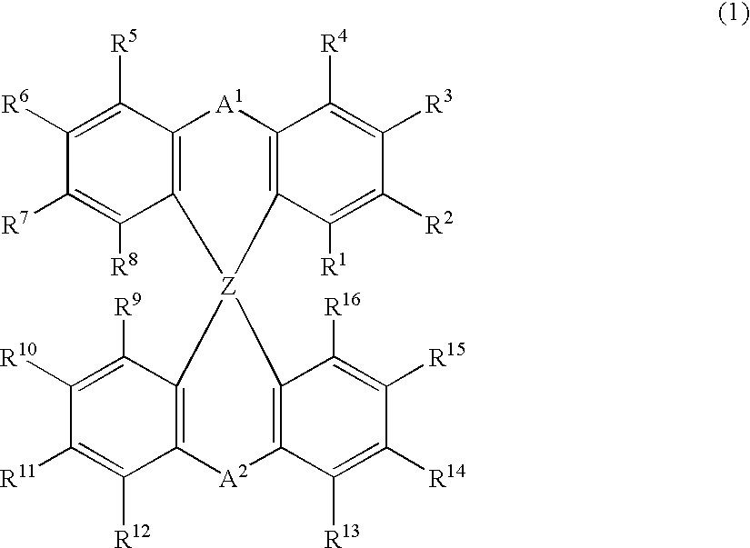
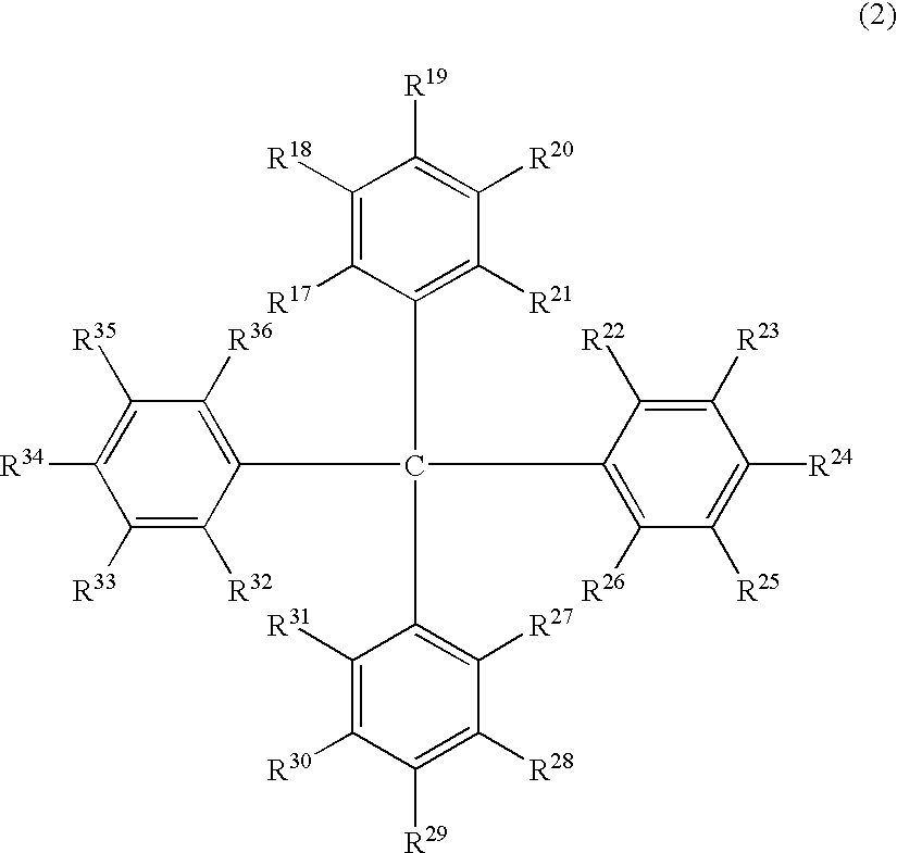
A light emitting device includes an emissive substance between an anode and cathode that emits light upon application of electrical energy. The emissive substance included in the device is at least one of the following types of compounds: (a) a compound having a plurality of 1,7-phenanthroline skeletal structures; (b) a benzoquinoline derivative; (c) a spiro compound; and (d) a tetraphenylmethane derivative.

Description

TECHNICAL FIELD[0001]The present invention relates to light emitting device materials and to a light emitting device which can convert electrical energy into light and can be used for display elements, flat panel displays, back lights, lighting, interiors, signs, signboards, electronic cameras, light signal generators and the like.TECHNICAL BACKGROUND[0002]There has recently been considerable research into organic multi-layered thin film light-emitting devices which emit light when electrons injected from a cathode and holes injected from an anode recombine within an organic fluorescent body interposed between the electrodes. Such devices are a focus of attention on account of their characteristics of thin shape, high luminance at low driving voltage and polychromic light emission based on suitable selection of the fluorescent materials.[0003]Numerous research organizations have been carrying out such research since C. W. Tang and co-workers at Kodak first described the fact that an...

Claims


Application Information

Patent Timeline
Patent Type & Authority Patents(United States)
IPC IPC(8): H01J1/62C07F9/02C07C15/28C07C15/52C07D209/14C07D209/86C07D213/53C07D215/12C07D219/02C07D221/10C07D235/20C07D241/42C07D249/08C07D263/32C07D263/62C07D263/64C07D271/10C07D271/107C07D277/66C07D311/96C07D405/14C07D407/14C07D409/14C07D413/14C07D417/14C07D519/00C07F7/08C07F9/38C07F9/6561C09K11/06H01L51/00H01L51/30H01L51/50
CPCC07C15/28C07C15/52C07D209/14C07D209/86C07D213/53C07D215/12C07D219/02C07D221/10C07D235/20C07D241/42C07D249/08C07D263/32C07D263/64C07D271/107C07D277/66C07D311/96C07D405/14C07D407/14C07D409/14C07D413/14C07D417/14C07F7/0807C07F7/0814C07F9/3813C07F9/6561C09K11/06H01L51/0036H01L51/0058H01L51/0067H01L51/0072H01L51/008H01L51/0094C09B11/04C09B11/12C09B11/28C09B23/0008C09B23/04C09B23/148C09B57/00C09B57/007C09B57/10C09K2211/1003C09K2211/1007C09K2211/1011C09K2211/1029C09K2211/1033C09K2211/1037C09K2211/1044C09K2211/1048C09K2211/1059C09K2211/1088C09K2211/1092C09K2211/1096H01L51/005H01L51/0059H01L51/007H01L51/0081H01L51/50H01L51/5012Y10S428/917H10K85/60H10K85/113H10K85/6565H10K85/626H10K85/631H10K85/322H10K85/324H10K85/654H10K85/6572H10K85/40H10K50/11H10K50/00H05B33/14C09K2211/1022
Inventor TOMINAGA, TSUYOSHIKITAZAWA, DAISUKEMAKIYAMA, AKIKOHAMA, AKIRA
Owner TORAY IND INC
Learn More