Nonvolatile memory utilizing asymmetric characteristics of hot-carrier effect

a technology of hot-carrier effect and non-volatile memory, which is applied in the field of memory circuits, can solve problems such as increasing manufacturing costs, and achieve the effect of efficient us

Active Publication Date: 2008-01-22
NSCORE
View PDF14 Cites 8 Cited by
  • Summary
  • Abstract
  • Description
  • Claims
  • Application Information

AI Technical Summary

Benefits of technology

[0011]It is another and more specific object of the present invention to provide a hot-carrier-effect-based nonvolatile semiconductor memory device that utilizes the asymmetric characteristic of a hot-carrier effect for the purpose of enhancing data-write speed.
[0015]According to at least one embodiment of the present invention, with the swapping of the source and drain nodes for the data read operation (second operation mode) relative to the data write operation (first operation mode), a change in the transistor characteristics caused by a hot-carrier effect is efficiently used as a means to store data. Further, since the first and second nodes of the latch are used as source nodes during the write operation (first operation mode), the potential that causes a hot-carrier effect is not applied to the transistors constituting the latch. With this arrangement, it is possible to avoid causing a hot-carrier effect to the transistors used in the latch circuit, and, thus, these transistors do not have to be designed to have a thicker gate oxide film that ensures hot-carrier-effect-free transistor operations even at high potentials. All the MIS transistors used in the memory cell (i.e., the MIS transistors serving as memory cell transistors and the MIS transistors constituting the latch circuit) may thus be properly designed to have the same structure with the same thickness of the gate oxide film.

Problems solved by technology

The need for such transistor having a special structure and the need for such film made of a special material are one of the factors that result in an increase in the manufacturing costs.

Method used


Image

  • Nonvolatile memory utilizing asymmetric characteristics of hot-carrier effect
  • Nonvolatile memory utilizing asymmetric characteristics of hot-carrier effect
  • Nonvolatile memory utilizing asymmetric characteristics of hot-carrier effect

Examples


first embodiment

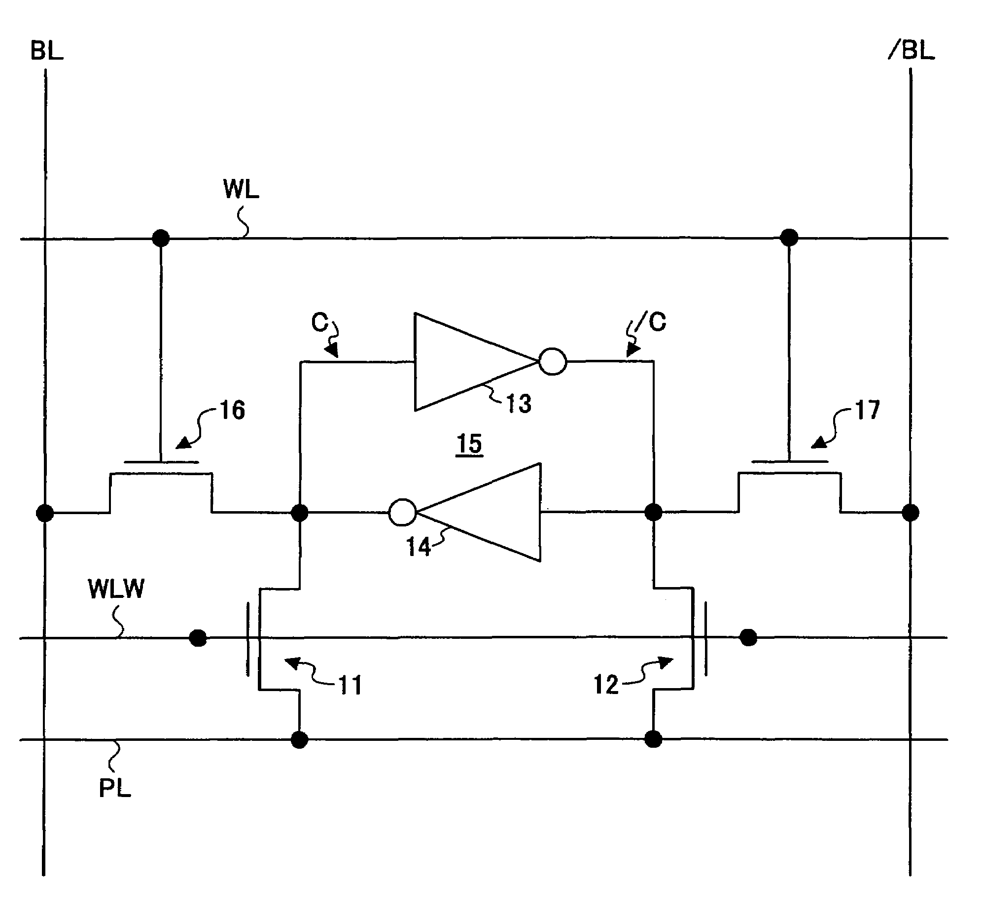
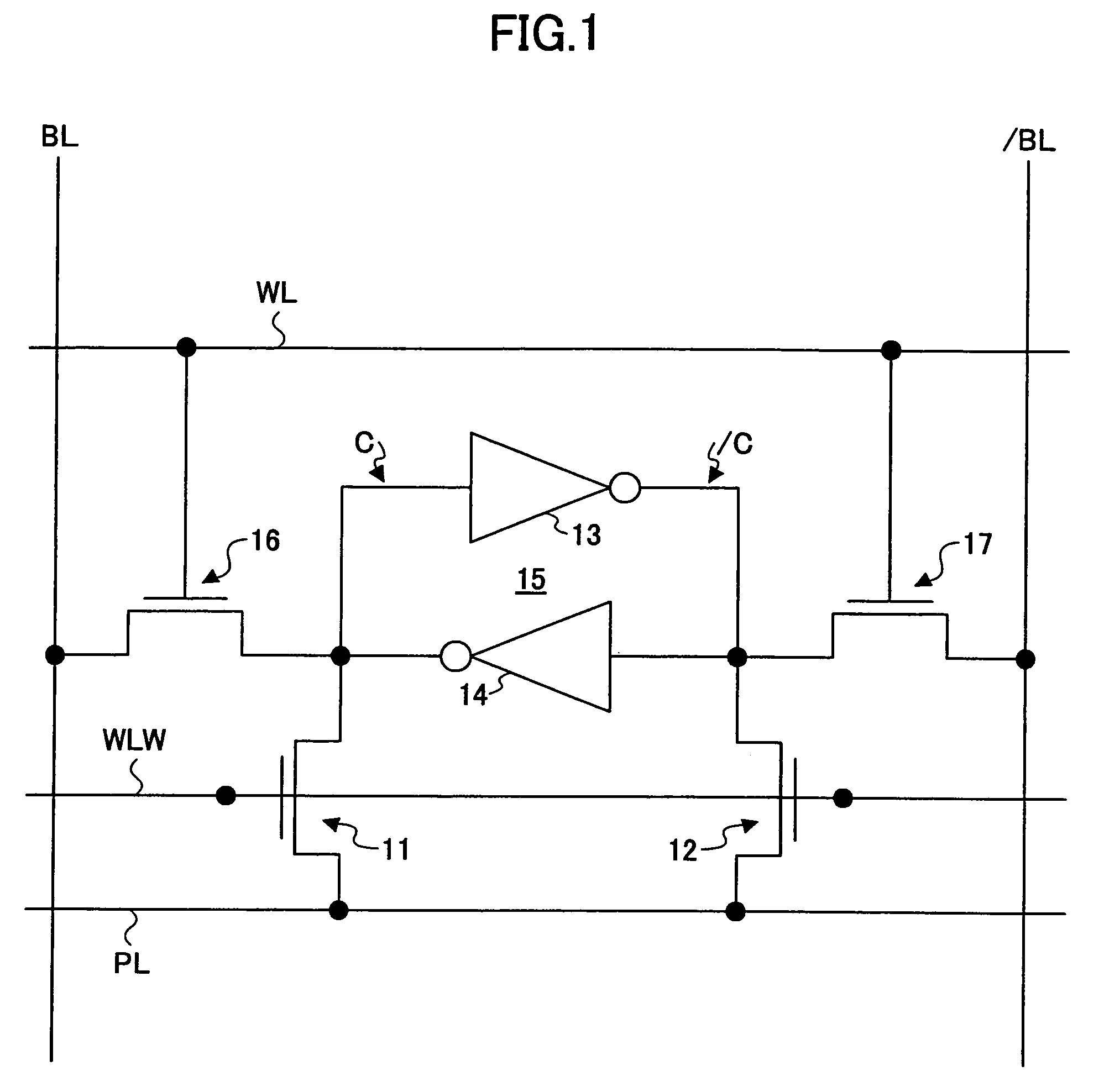
[0075]FIG. 4 is an illustrative drawing showing the configuration of a memory cell according to the nonvolatile memory device of the present invention.

[0076]The memory cell includes NMOS transistors 51 and 52, a PMOS transistor 53, NMOS transistors 54 through 56, PMOS transistors 57 and 58, and NMOS transistors 59 and 60. The NMOS transistors 54 and 56 and PMOS transistors 57 and 58 together constitute a volatile memory unit, which corresponds to the latch circuit 15 of the memory cell shown in FIG. 1. The NMOS transistors 51 and 52 correspond to the NMOS transistors 11 and 12 shown in FIG. 1, constituting a nonvolatile memory unit.

[0077]The NMOS transistors 11 and 12 serving as nonvolatile memory cell transistors have the same structure as the other NMOS transistors including the NMOS transistors 54 through 56 used in the volatile memory unit and the NMOS transistors 59 and 60 used as a transfer gate between the memory cell and the bit lines. Further, it is preferable to manufactur...

second embodiment

[0100]FIG. 11 is an illustrative drawing showing the configuration of a memory cell according to the nonvolatile memory device of the present invention. The same elements as those of FIG. 4 are referred to by the same numerals, and a description thereof will be omitted unless necessary.

[0101]The memory cell includes an NMOS transistor 62 and a PMOS transistor 63, in addition to the NMOS transistors 51 and 52, the PMOS transistor 53, the NMOS transistors 54 through 56, the PMOS transistors 57 and 58, and the NMOS transistors 59 and 60 that are the same transistors as shown in FIG. 4. The NMOS transistor 62 and the PMOS transistor 63 have a thicker gate oxide film than the other transistors, so that they are designed to operate in the 0-to-3.3 voltage range

[0102]As shown in FIG. 11, there is no plate line PL in the second embodiment. A store line STORE is provided to extend from the row signal driver 48, and is coupled to the gate node of the PMOS transistor 63. A signal line providin...

third embodiment

[0127]FIG. 19 is an illustrative drawing showing the configuration of a memory cell according to the nonvolatile memory device of the present invention. The same elements as those of FIG. 11 are referred to by the same numerals, and a description thereof will be omitted unless necessary.

[0128]The configuration shown in FIG. 19 differs from that of FIG. 11 only in that the signal line RECALL and the store line STORE extend in a direction perpendicular to the word selecting line WLW. In FIG. 19, the signal line that is coupled to the gate of the NMOS transistor 62 is denoted as RECALL1, and the signal line that is coupled to the gate of the PMOS transistor 63 is denoted as STORE1.

[0129]This configuration makes it possible to select a single memory cell for the store operation and the restore operation by achieving a row selection by WLW and a column selection by RECALL and STORE. Namely, a bit-by-bit store operation as well as a bit-by-bit restore operation can be performed.


PUM


Abstract

A memory circuit includes a latch having a first node and a second node, a first MIS transistor having source / drain nodes thereof coupled to the first node and to a plate line, respectively, and a gate node thereof coupled to a word selecting line, a second MIS transistor having source / drain nodes thereof coupled to the second node and to the plate line, respectively, and a gate node thereof coupled to the word selecting line, and a driver circuit configured to set the plate line to a first potential causing the first node to serve as a source node of the first MIS transistor in a first operation mode and to a second potential causing the first node to serve as a drain node of the first MIS transistor in a second operation mode, the first operation mode causing a lingering change in characteristics of the first MIS transistor.

Description

BACKGROUND OF THE INVENTION[0001]1. Field of the Invention[0002]The present invention generally relates to a memory circuit, and particularly relates to a nonvolatile memory circuit which is capable of retaining stored data in the absence of a power supply voltage.[0003]2. Description of the Related Art[0004]Nonvolatile semiconductor memory devices, which can retain stored data even when power is turned off, include flash EEPROMs employing a floating gate structure, FeRAMs employing a ferroelectric film, MRAMs employing a ferromagnetic film, etc.[0005]In the case of EEPROMs, there is a need to manufacture a transistor having a special structure comprised of a floating gate. In the case of FeRAMs and MRAMs, which achieve nonvolatile storage by use of a ferroelectric material and a ferromagnetic material, respectively, there is a need to form and process a film made of these respective materials. The need for such transistor having a special structure and the need for such film made o...

Claims


Application Information

Patent Timeline
Patent Type & Authority Patents(United States)
IPC IPC(8): G11C11/00
CPCG11C7/1045G11C8/08G11C14/00G11C14/0063
Inventor NODA, KENJI
Owner NSCORE
Why Eureka
Try Eureka