
Piezoelectric thin film device and method for manufacturing the same

a thin film, piezoelectric technology, applied in piezoelectric/electrostrictive/magnetostrictive devices, relays, generators/motors, etc., can solve the problem of small electromechanical coupling constant, difficult to correspond to recent higher usage frequency demands, orientation of piezoelectric films, etc., to achieve the effect of electromechanical coupling constan

Inactive Publication Date: 2008-01-29
KK TOSHIBA
View PDF15 Cites 31 Cited by
  • Summary
  • Abstract
  • Description
  • Claims
  • Application Information

AI Technical Summary

Benefits of technology

[0014]It is an object of the present invention to provide a piezoelectric thin film device having an electromechanical coupling constant that can be improved, as well as a manufacturing method for the same.

Problems solved by technology

Since, at a frequency range exceeding 1 GHz, the gap distance between comb type electrodes of SAW devices is 1 m or less, it is difficult to correspond to recent higher usage frequencies demands.
However, there are limits on the orientation of the AlN piezoelectric film formed on top of the sacrificial layer, which raises the problem of a small electromechanical coupling constant.
It may be a problem to use the (111) orientated substrate, which is different from the (100) orientated substrate used in general manufacturing methods of semiconductor devices.
Because volume contraction occurs due to the annealing, the residual distortion of the PZT film will inevitably increase.
Therefore, it is difficult to suppress warpage occurring on the PZT piezoelectric film by residual distortion.
Therefore, it is possible to have a small electromechanical coupling constant of the piezoelectric film, which may not be sufficient to ensure a sufficient drive range of the piezoelectric actuator.

Method used


Image

  • Piezoelectric thin film device and method for manufacturing the same
  • Piezoelectric thin film device and method for manufacturing the same
  • Piezoelectric thin film device and method for manufacturing the same

Examples


first embodiment

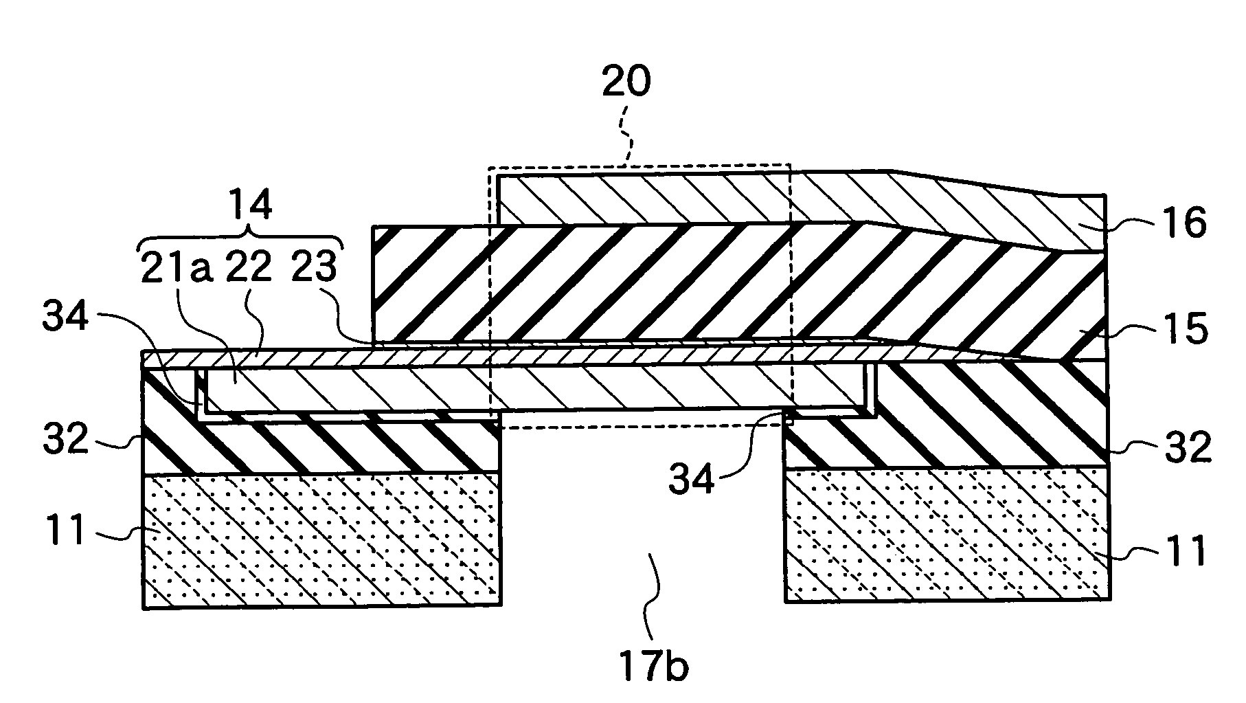
[0061]An FBAR as a piezoelectric thin film device according to a first embodiment of the present invention includes a bottom electrode 14 of an amorphous metal film provided on a surface of a substrate 11, a piezoelectric film 15 provided on a surface of the bottom electrode 14, and a top electrode (top metal film) 16 provided on top of a surface of the piezoelectric film 15, as shown in FIG. 5. A resonator 20 is defined as a region in which the bottom electrode 14 and the top electrode 16 are facing each other, including the piezoelectric film 15 sandwiched by the facing bottom electrode 14 and top electrode 16.

[0062]Additionally, as shown in FIG. 6, a barrier layer 13 is provided surrounding a cavity 17 provided on top of the substrate 11. The resonator 20 is disposed on top of the cavity 17 so as to be projecting into a free space. The bottom electrode 14 is provided from the surface of the substrate 11 extending to the surface of the barrier layer 13. For example, the substrate ...

second embodiment

[0171]A variable capacitor as a piezoelectric thin film device according to a second embodiment of the present invention includes a piezoelectric actuator 40 and a fixed electrode 46, as shown in FIG. 56. As shown in FIG. 57, a fixed end portion (first end portion) 48 of the piezoelectric actuator 40 is held on an anchor 42 provided on a surface of an insulating film 32 on a substrate 11. A working end portion (second end portion) 49 of the piezoelectric actuator 40 is projecting into a free space so as to face the fixed electrode 46 placed on the surface of the insulating film 32.

[0172]The piezoelectric actuator 40 includes a bottom electrode 14, a piezoelectric film 15, a top electrode 16, and a supporting film. The bottom electrode 14 is provided to extend to a location above the fixed electrode 46 from a surface of the anchor 42. The piezoelectric film 15 is placed on a surface of the bottom electrode 14. The top electrode 16 faces the bottom electrode 14 to sandwich the piezoel...


PUM

PropertyMeasurementUnit
resistivityaaaaaaaaaa
thicknessaaaaaaaaaa
root mean square roughnessaaaaaaaaaa

Abstract

A piezoelectric thin film device includes an amorphous metal film disposed on a substrate and a piezoelectric film disposed on the amorphous metal. One of crystal axis of the piezoelectric film is aligned in a direction perpendicular to a surface of the amorphous metal.

Description

CROSS REFERENCE TO RELATED APPLICATIONS AND INCORPORATION BY REFERENCE[0001]This application is based upon and claims the benefit of priority from prior Japanese patent application P2004-020132 filed on Jan. 28, 2004, P2005-001346 filed on Jan. 6, 2005, and P2005-007850 filed on Jan. 14, 2005; the entire contents of which are incorporated by reference herein.BACKGROUND OF THE INVENTION[0002]1. Field of the Invention[0003]The present invention relates to piezoelectric thin film devices used in piezoelectric devices, and particularly to piezoelectric thin film devices used in high frequency bands, and a manufacturing method for the same.[0004]2. Description of the Related Art[0005]Recently, high frequency bands in the GHz range are being used in wireless communication systems such as mobile communication devices, and local area network (LAN) systems transferring data between computers at high transfer rates. Piezoelectric thin film devices are receiving attention in applications such ...

Claims


Application Information

Patent Timeline
Patent Type & Authority Patents(United States)
IPC IPC(8): H01L41/047H01L41/22H03H3/02H03H9/02H03H9/15H03H9/17
CPCH01L41/316H03H3/02H03H9/02015H03H9/02094H03H9/173H03H9/174H03H9/175H03H9/542H03H9/582H03H9/605H01L41/047H01H2057/006Y10T29/49155H03H2003/021H03H2003/023H03H2003/025Y10T29/42Y10T29/435Y10T29/49005Y10T29/49117Y10T29/49002H10N30/877H10N30/2042H10N30/079H10N30/076
Inventor SANO, KENYAOHARA, RYOICHIYANASE, NAOKOYASUMOTO, TAKAAKIITAYA, KAZUHIKOKAWAKUBO, TAKASHITOYODA, HIROSHIHASUNUMA, MASAHIKONAGANO, TOSHIHIKOABE, KAZUHIDENISHIGAKI, MICHIHIKOSHIBATA, HIRONOBU
Owner KK TOSHIBA
Learn More