Semiconductor device

a technology of semiconductor devices and driver circuits, which is applied in semiconductor devices, digital storage, instruments, etc., can solve the problems of increased time constants of word lines, increased number of sub-word driver circuits (swd), and delay in access time (trcd)

Inactive Publication Date: 2008-01-24
ELPIDA MEMORY INC
View PDF11 Cites 29 Cited by
  • Summary
  • Abstract
  • Description
  • Claims
  • Application Information

AI Technical Summary

Problems solved by technology

As a result, the time constant (RC) of the word line is increased, and delay is caused in access time (tRCD) from an active command to a read command.
However, although the access time (tRCD) can be speeded up when the word line length is shortened, there are problems that the number of sub word driver circuits (SWD) is increased since the number of division of a memory array is increased, and the chip size is thus increased.

Method used


Image

  • Semiconductor device
  • Semiconductor device
  • Semiconductor device

Examples


Embodiment Construction

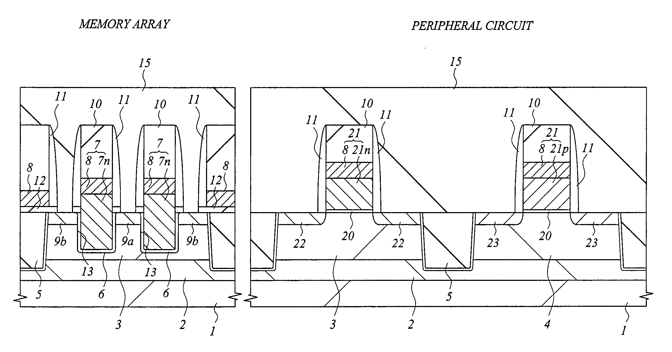
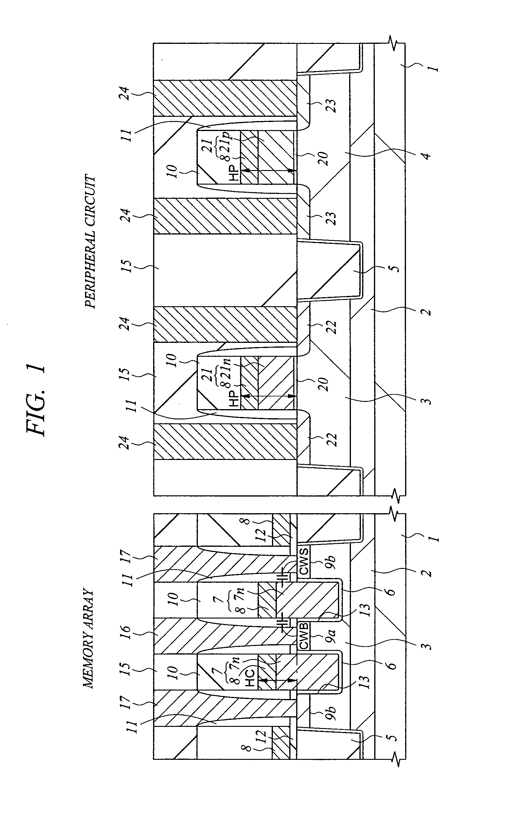
[0051]Hereinafter, embodiments of the present invention will be described in detail with reference to the accompanying drawings. Note that components having the same function are denoted by the same reference symbols throughout the drawings for describing the embodiment, and the repetitive description thereof will be omitted.

[0052]Although not limited to this, as a transistor configuring each block described in the embodiments, the transistor is formed on a single crystal silicon substrate by using an integrated circuit technique such as a known CMOS transistor (complementary MOS transistor) manufacturing technique. More specifically, the transistor is formed by a process including a step of forming a gate electrode and semiconductor regions constituting source and drain regions after forming a well, an isolation region, and a gate insulating film.

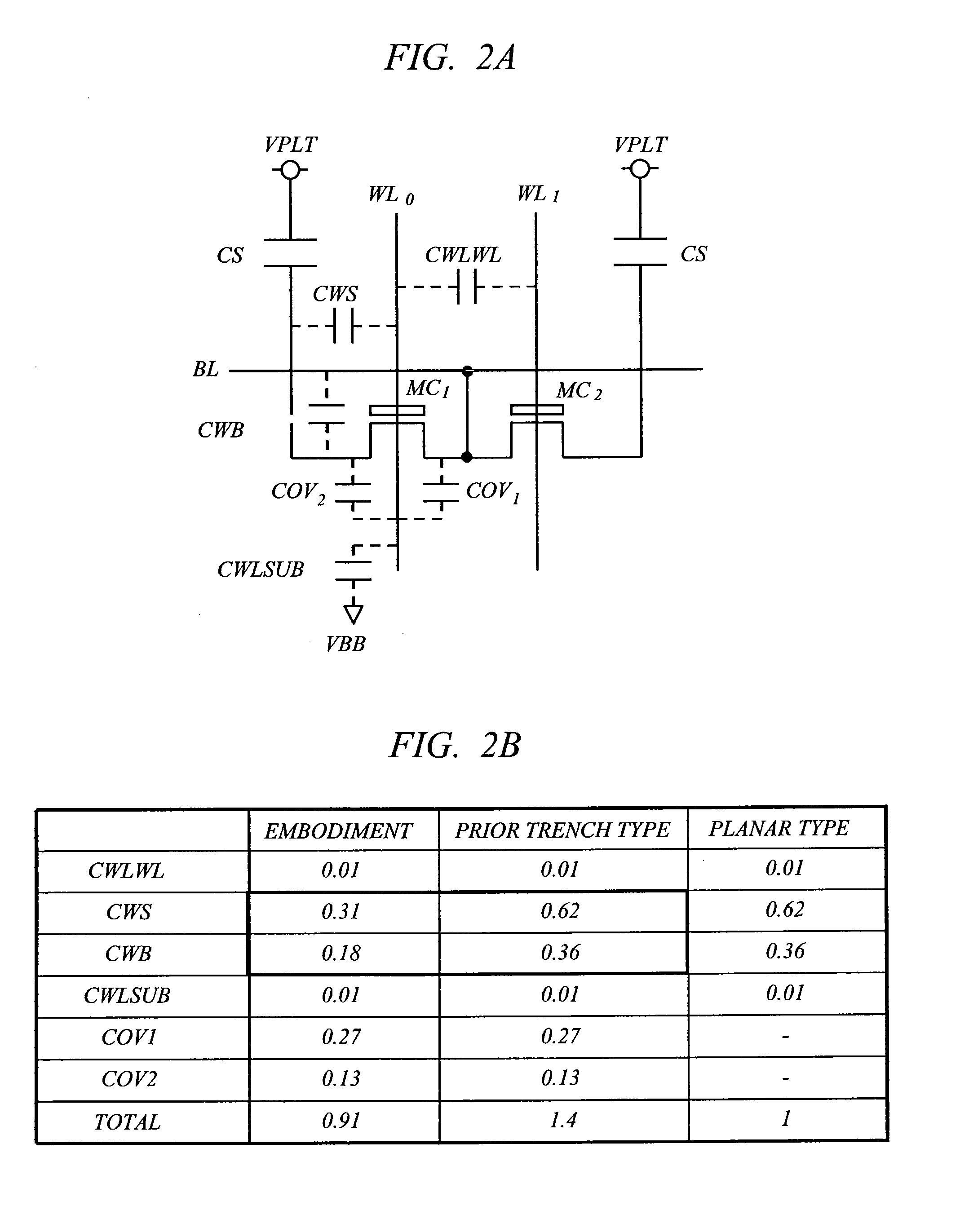
[0053]A circuit symbol of a MOSFET (Metal Oxide Semiconductor Field Effect Transistor) with a circle at a gate represents p-channel type ...


PUM


Abstract

A DRAM capable of realizing reduced power consumption, high-speed operation, and high reliability is provided. A gate electrode configuring a memory cell transistor of the DRAM is composed of an n-type polysilicon film and a W (tungsten) film stacked thereon. A part of the polysilicon film is embedded in a trench formed in a silicon substrate in order to elongate the effective channel length of the memory cell transistor. The other part of the polysilicon film is located above the trench, and an upper surface thereof is located above a surface of the silicon substrate (p-type well). Therefore, distances between the W film and a source and drain (n-type semiconductor regions) are ensured.

Description

CROSS-REFERENCE TO RELATED APPLICATION[0001]The present application claims priority from Japanese Patent Application No. JP 2006-197602 filed on Jul. 20, 2006, the content of which is hereby incorporated by reference into this application.TECHNICAL FIELD OF THE INVENTION[0002]The present invention relates to a semiconductor device and a technique for manufacturing thereof. More particularly, the present invention relates to a technique effectively applied to a semiconductor device comprising Dynamic Random Access Memory (hereinafter, referred to as DRAM).BACKGROUND OF THE INVENTION[0003]Dynamic Random Access Memory (hereinafter, referred to as DRAM), which is a kind of semiconductor memory devices, is mounted on a number of various electronic devices we use in daily life. Further, along with the needs for reduction in power consumption and enhanced performance of recent devices, enhancement in performance such as reduction in power consumption, speed-up, and increase in the capacity...

Claims


Application Information

Patent Timeline
Patent Type & Authority Applications(United States)
IPC IPC(8): H01L27/108H01L21/8242
CPCG11C7/18G11C11/404G11C11/4097H01L27/10876H01L27/10891H01L2924/0002H01L27/10894H01L29/66621H01L2924/00H10B12/053H10B12/488H10B12/09
Inventor AKIYAMA, SATORUTSUCHIYA, RYUTASEKIGUCHI, TOMONORITAKEMURA, RIICHIRONAKAMURA, MASAYUKIYAMAZAKI, YASUSHISHIRATAKE, SHIGERU
Owner ELPIDA MEMORY INC
Why Eureka
Try Eureka